
Circuit timing analysis incorporating the effects of temperature inversion

a technology of circuit timing and temperature inversion, applied in the field of circuit timing analysis and design, can solve the problems of increasing cell delay with increasing temperature, reducing cell delay, and temperature dependence not being uniform for all cells, and achieve the effect of improving the accuracy of circuit timing characterization

Active Publication Date: 2012-05-15
BELL SEMICON LLC
View PDF12 Cites 13 Cited by
  • Summary
  • Abstract
  • Description
  • Claims
  • Application Information

AI Technical Summary

Benefits of technology

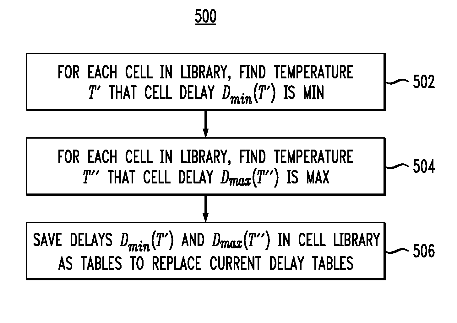
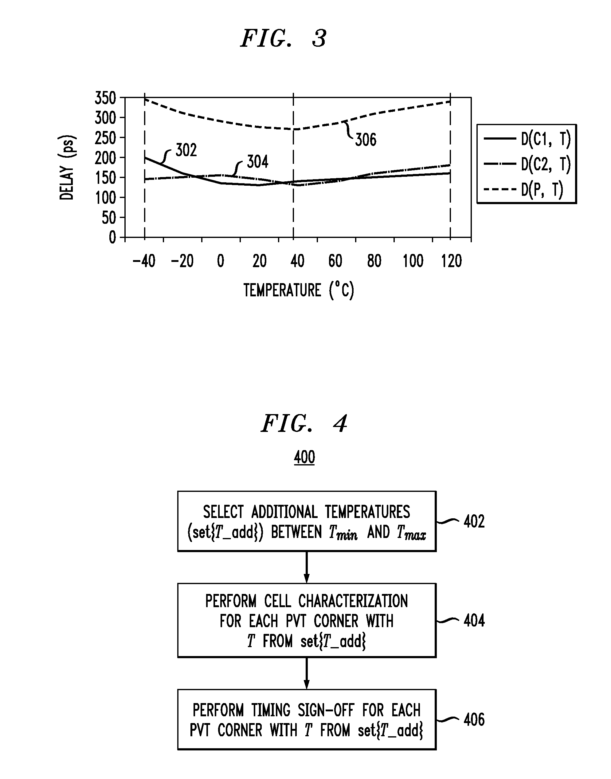
"The present invention provides techniques for improving the accuracy of circuit timing characterization. This is achieved by performing cell library timing characterization for each cell in the circuit for at least first and second prescribed temperatures, calculating cell delays for each cell as a function of temperature, and incorporating the cell delay calculation into the timing characterization for each cell. Additionally, the invention includes methods for determining minimum and maximum temperatures for each cell, performing circuit simulation on timing critical paths, and determining timing margins to increase the accuracy of the timing characterization of the circuit. These techniques can be implemented in an apparatus including memory and at least one processor."

Problems solved by technology

Many challenges affect the ability to accurately predict the performance of circuit designs, particularly as integrated circuit (IC) fabrication process technologies migrate into sub-100 nanometer (nm) regions.
Such challenges include, for example, circuit complexity, process variability and uncertainty, modeling uncertainty, variability in assumptions utilized in electronic design automation (EDA) tools, etc.
However, newer modeling obstacles, with varying degrees of influence, are becoming critical in achieving silicon accuracy in both analysis and implementation.
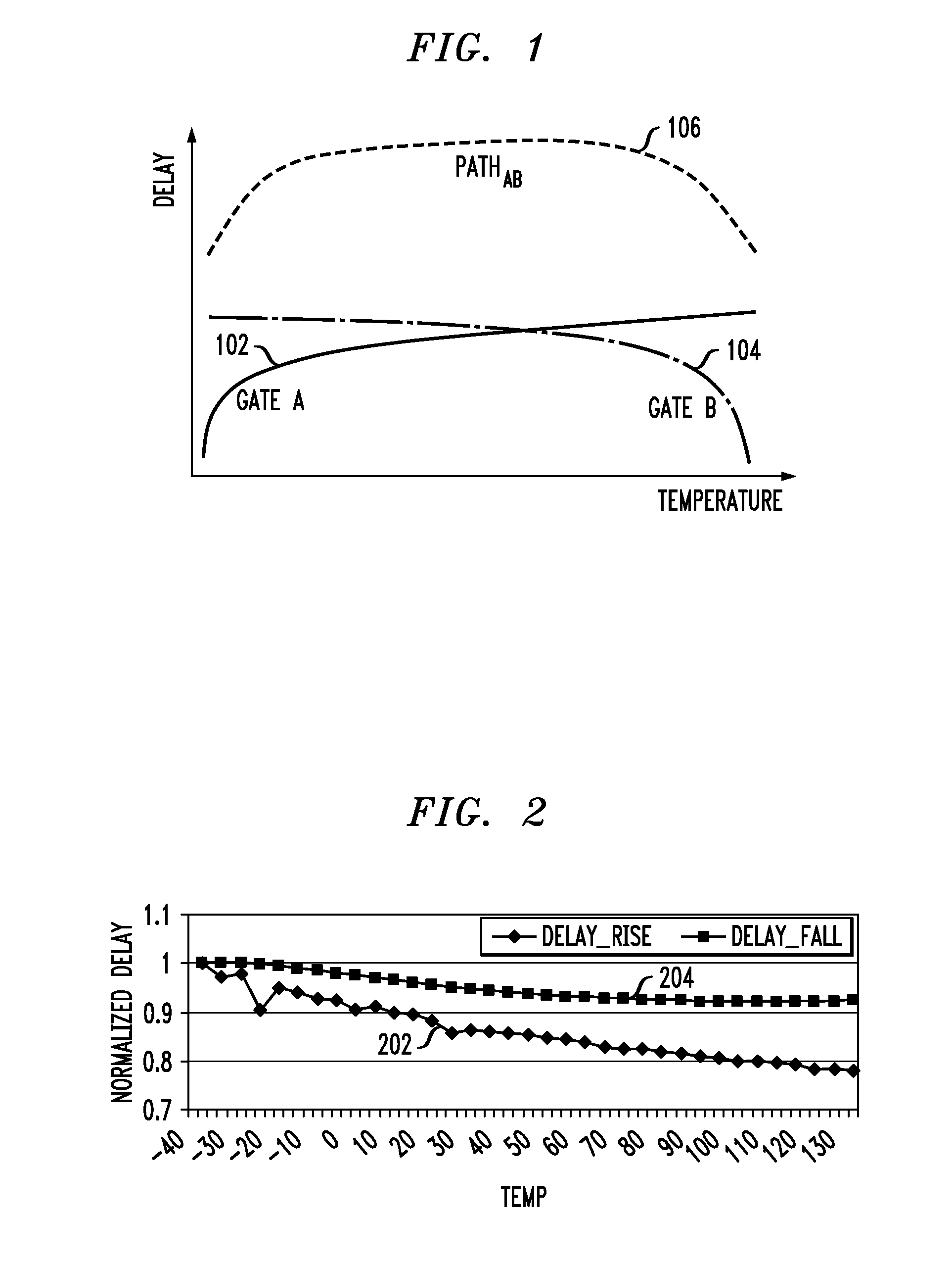
Traditionally, cell delay increases with rising temperature.
But in sub-100nm process designs, measurement has shown that cell delays can decrease with rising temperature.
At sub-100 nm, it has been observed that the extent of temperature dependency can vary differently with each type of cell and its load in the circuit, and such temperature dependency need not be uniform for all cells.
Conventional modeling and analysis tools have proved to be inadequate in terms of predicting circuit behavior for sub-100 nm process designs.

Method used


Image

  • Circuit timing analysis incorporating the effects of temperature inversion
  • Circuit timing analysis incorporating the effects of temperature inversion
  • Circuit timing analysis incorporating the effects of temperature inversion

Examples


Embodiment Construction

[0023]The present invention will be described herein in the context of exemplary techniques for more accurately determining cell and / or path delay in a circuit. It is to be understood, however, that the techniques of the present invention are not limited to the methodologies shown and described herein. Rather, embodiments of the invention are directed to techniques for advantageously predicting timing behavior in a circuit taking into account temperature inversion effects. In this manner, a more accurate determination of cell and / or path delay in the circuit can be achieved. Although reference may be made herein to n-channel metal-oxide-semiconductor (NMOS) or p-channel metal-oxide-semiconductor (PMOS) transistor devices which may be formed using a complementary metal-oxide-semiconductor (CMOS) IC fabrication process, the invention is not limited to such devices and / or such an IC fabrication process.

[0024]Inverted temperature dependence (ITD), also referred to herein as temperature ...


PUM


Abstract

Methods and apparatus for increasing the accuracy of timing characterization of a circuit including one or more cells in a cell library are provided. One method includes the steps of: performing cell library timing characterization for each of the cells in the circuit for at least first and second prescribed temperatures, the first and second temperatures corresponding to first and second PVT corners, respectively, in the cell library; calculating respective cell delays for the one or more cells in the circuit, the cell delay calculation being a function of temperature for each instance of the one or more cells; and incorporating the cell delay calculation into the timing characterization for each of the cells in the circuit to thereby increase the accuracy of the timing characterization.

Description

CROSS-REFERENCE TO RELATED APPLICATION(S)[0001]The present application is related to a commonly assigned U.S. application Ser. No. 12 / 251,110 entitled “Reducing Path Delay Sensitivity to Temperature Variation in Timing-critical Paths,” and filed on even date herewith, the disclosure of which is incorporated by reference herein in its entirety.FIELD OF THE INVENTION[0002]The present invention relates generally to the electrical, electronic, and computer arts, and more particularly relates to circuit timing analysis and design.BACKGROUND OF THE INVENTION[0003]Many challenges affect the ability to accurately predict the performance of circuit designs, particularly as integrated circuit (IC) fabrication process technologies migrate into sub-100 nanometer (nm) regions. Such challenges include, for example, circuit complexity, process variability and uncertainty, modeling uncertainty, variability in assumptions utilized in electronic design automation (EDA) tools, etc. In order to compens...

Claims


Application Information

Patent Timeline
Patent Type & Authority Patents(United States)
IPC IPC(8): G06F17/50
CPCG06F17/5031G06F17/5068G06F2217/84G06F30/3312G06F2119/12G06F30/39G06F30/3315
Inventor TETELBAUM, ALEXANDER
Owner BELL SEMICON LLC
Learn More