Liquid crystal display panel with microlens array, its manufacturing method, and liquid crystal display device

a liquid crystal display panel and microlens array technology, applied in the field of liquid crystal display panel and liquid crystal display device, can solve the problems of reducing the contrast ratio, reducing the resistance of elements in an off state, and unable to obtain predetermined display states, so as to prevent material chipping and cracking, reduce production costs, and reduce production costs.

Inactive Publication Date: 2012-05-08
SHARP KK
View PDF237 Cites 0 Cited by
  • Summary
  • Abstract
  • Description
  • Claims
  • Application Information

AI Technical Summary

Benefits of technology

[0046]According to the present invention, the wiring connection substrate is mounted to a portion (overhang) of the electrical element substrate where the support is not formed, thereby preventing chipping and cracking of the material, which might occur in a step of mounting the flexible printed wiring board. As a result, there are provided a high-quality liquid crystal display panel with a microlens array and a liquid crystal display device which have a good production efficiency and experience little problem in the production steps. Moreover, according to the present invention, there is provided a method for efficiently producing such a liquid crystal display panel and liquid crystal display device.

Problems solved by technology

On the other hand, in a liquid crystal display device of the active matrix type, when strong light enters a switching element particular a TFT) which is provided on the display panel, its element resistance in an OFF state is decreased, thereby allowing the electric charge which was charged to the pixel capacitor under an applied voltage to be discharged, such that a predetermined displaying state cannot be obtained.
Thus, there is a problem of light leakage even in a black state, thus resulting in a decreased contrast ratio.
However, in a liquid crystal display device which performs displaying by utilizing transmitted light, providing a light shielding layer in addition to the TFTs, gate bus lines, and source bus lines, which do not transmit light, will allow the effective pixel area to be decreased, thus resulting in a decrease in the ratio of the effective pixel area to the total area of the displaying region, i.e., the aperture ratio.
The reason is that, even if there is a desire to reduce the pixel pitch, constraints such as electrical performance and fabrication techniques make it impossible for the TFTs, the bus lines, etc., to become smaller than certain sizes.
Thus, although transflective-type liquid crystal display devices have the advantage of realizing displaying with a high contrast ratio irrespective of the ambient brightness, they have a problem in that their brightness is lowered as the aperture ratio of the transmission region becomes smaller.

Method used


Image

  • Liquid crystal display panel with microlens array, its manufacturing method, and liquid crystal display device
  • Liquid crystal display panel with microlens array, its manufacturing method, and liquid crystal display device
  • Liquid crystal display panel with microlens array, its manufacturing method, and liquid crystal display device

Examples


Embodiment Construction

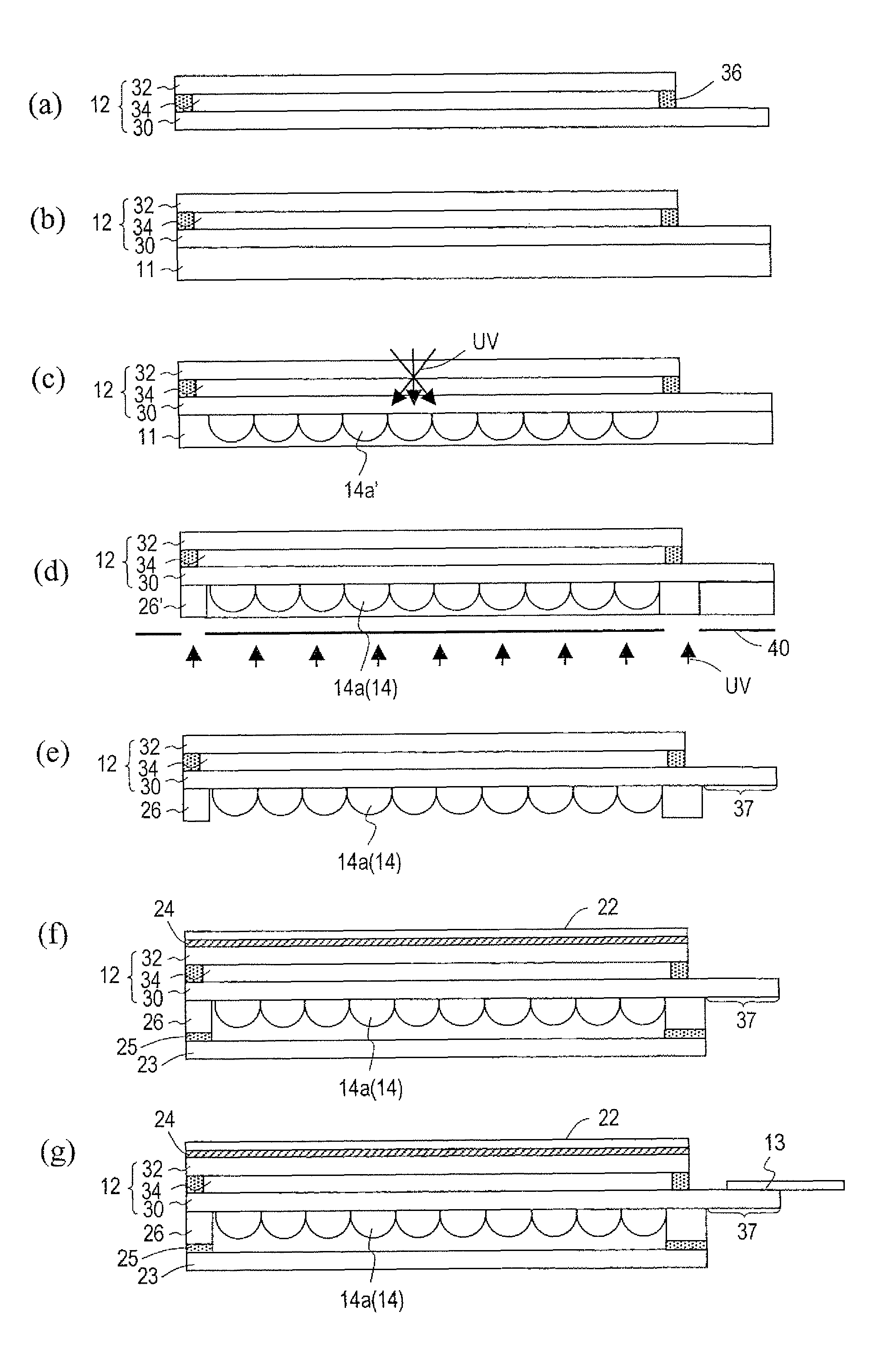
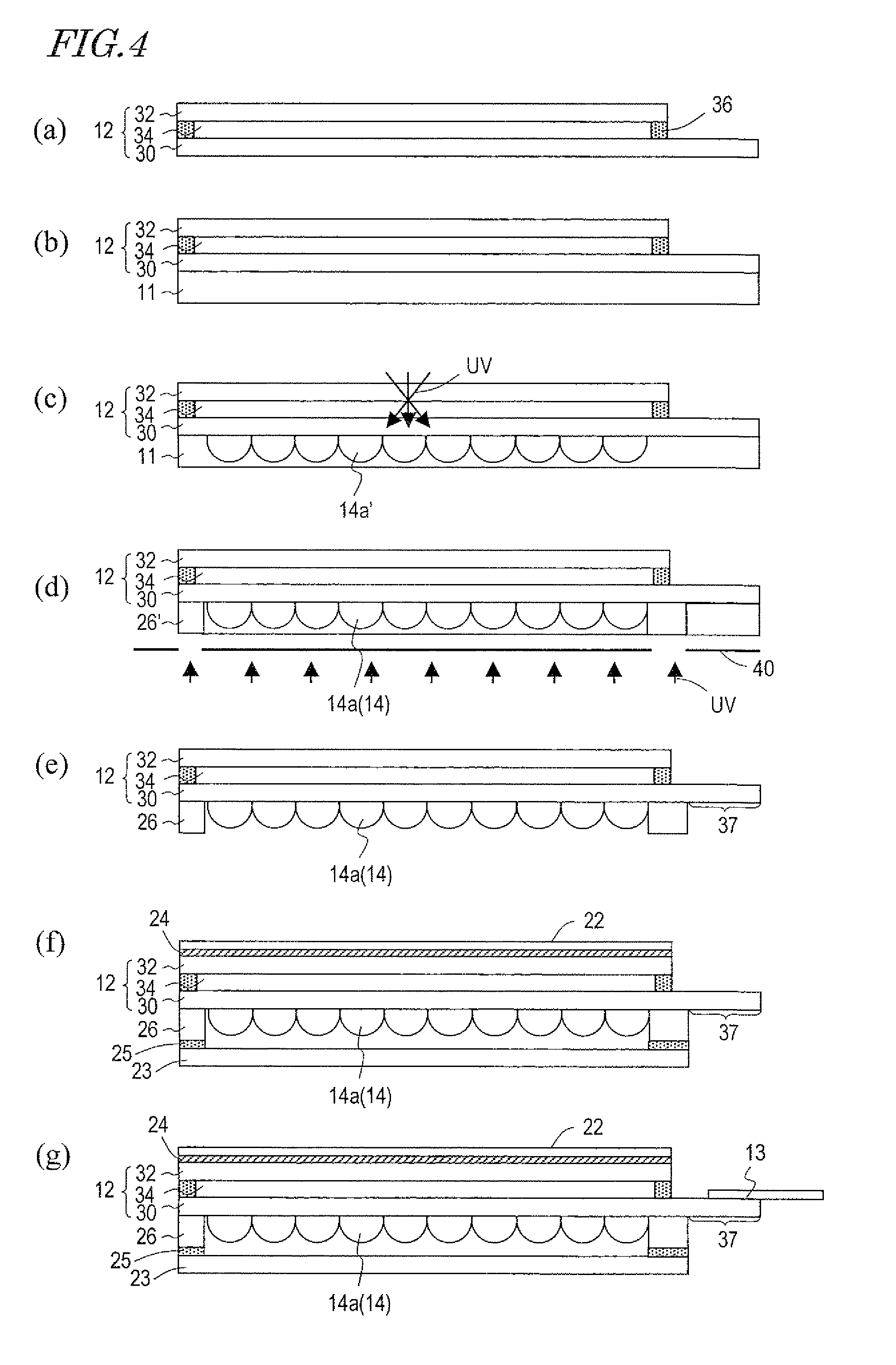
[0075]Hereinafter, with reference to the drawings, the structure of a liquid crystal display panel with a microlens array according to an embodiment of the present invention will be described.

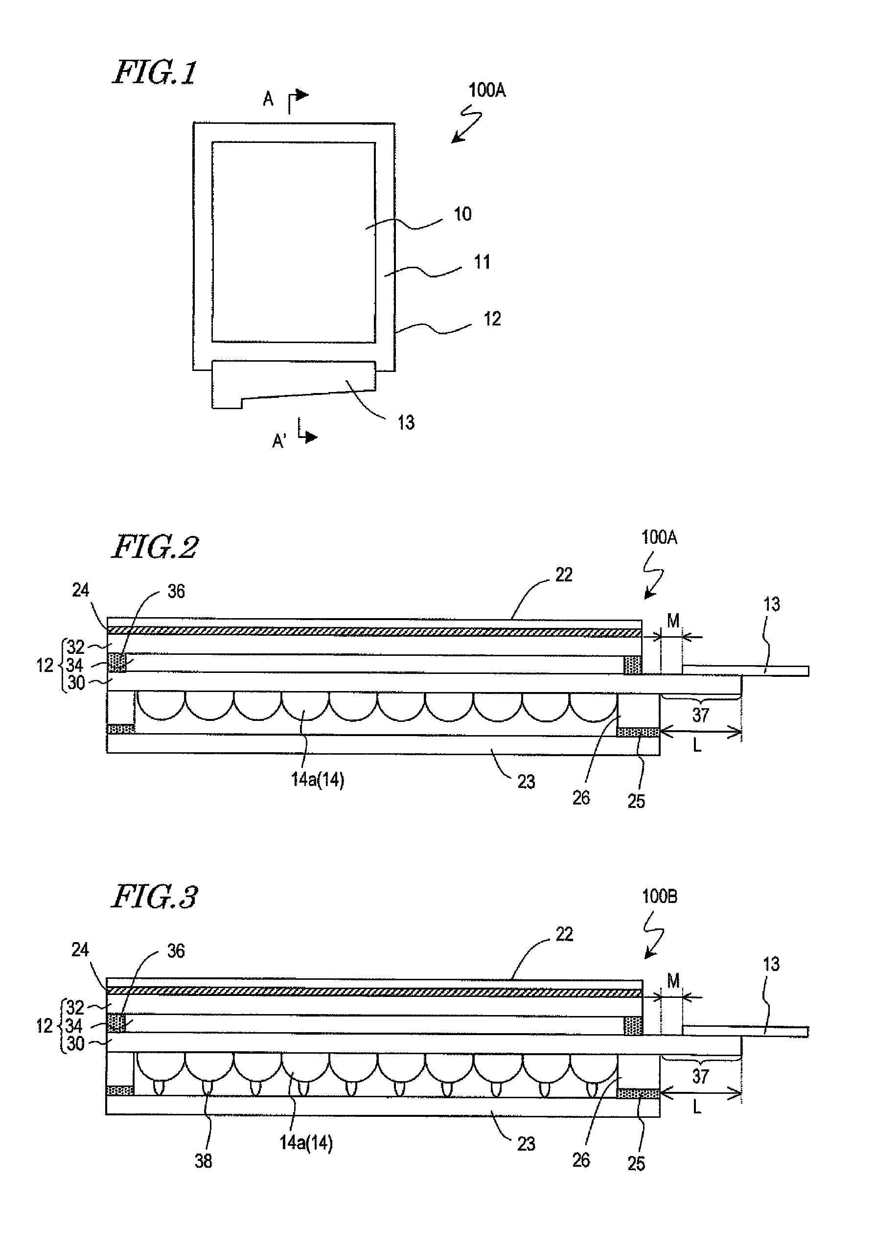
[0076]FIG. 1 is a plan view schematically showing the liquid crystal display panel with a microlens array of the present embodiment. FIG. 2 is a cross-sectional view showing the construction of the liquid crystal display panel with a microlens array of the present embodiment along an A-A′ cross section in FIG. 1.

[0077]As shown in FIG. 1, the liquid crystal display panel 100A with a microlens array of the present embodiment includes: a liquid crystal display panel (also referred to as the “liquid crystal cell”) 12, which includes a displaying region 10 having a plurality of pixels in a matrix arrangement and a peripheral region 11 around it; and a flexible printed wiring board (also referred to as the flexible printed circuit (FPC)) 13, which is a wiring connection substrate. The flexible printe...


PUM

PropertyMeasurementUnit
distanceaaaaaaaaaa
distanceaaaaaaaaaa
distanceaaaaaaaaaa

Abstract

A liquid crystal display panel according to the present invention includes: a liquid crystal display panel including an electrical element substrate on which switching elements for controlling the light transmittance of a liquid crystal layer are formed so as to respectively correspond to pixels; a microlens array provided on a light-incident side of the liquid crystal display panel; a support provided on the light-incident side of the liquid crystal display panel so as to be in a peripheral region of the microlens array; a rear-face side optical film attached to the liquid crystal display panel via the support; and a wiring connection substrate mounted to the electrical element substrate. The electrical element substrate includes an overhang which projects from the support in the direction of the wiring connection substrate, and the wiring connection substrate is mounted to the overhang.

Description

[0001]This application is the U.S. national phase of International Application No. PCT / JP2007 / 066658, filed 28 Aug. 2007, which designated the U.S. and claims priority to Japanese Patent Application No. 2006-264303, filed 28 Sep. 2006, the entire contents of each of which are hereby incorporated by reference.TECHNICAL FIELD[0002]The present invention relates to a liquid crystal display panel and a liquid crystal display device, and more particularly to a liquid crystal display panel which include a microlens array and a production method thereof.BACKGROUND ART[0003]In recent years, liquid crystal display devices are widely used as display devices for monitors, projectors, mobile information terminals, mobile phones, and the like. Generally speaking, a liquid crystal display device allows the transmittance (or reflectance) of a liquid crystal display panel to vary with a driving signal, thus modulating the intensity of light from a light source for irradiating the liquid crystal disp...

Claims


Application Information

Patent Timeline
Patent Type & Authority Patents(United States)
IPC IPC(8): G02F1/1335G02B27/10
CPCG02F1/133526G02F1/13452G02B3/0006G02B27/2214G02F1/133528G02F1/133567G02B30/27
Inventor KOSEGAWA, SEISHIUSUKURA, NARUMURAO, TAKEHIRO
Owner SHARP KK
Why Eureka
Try Eureka