Two terminal quantum device using MOS capacitor structure
a capacitor structure and quantum well technology, applied in semiconductor devices, instruments, electrical devices, etc., can solve problems such as problems such as problems such as the problem of integrating quantum well devices in silicon integrated circuits with energy level separations greater than 50 mev to allow operation at room temperature, and achieve the effect of facilitating filling the quantum well
- Summary
- Abstract
- Description
- Claims
- Application Information
AI Technical Summary
Benefits of technology
Problems solved by technology
Method used
Image
Examples
first embodiment
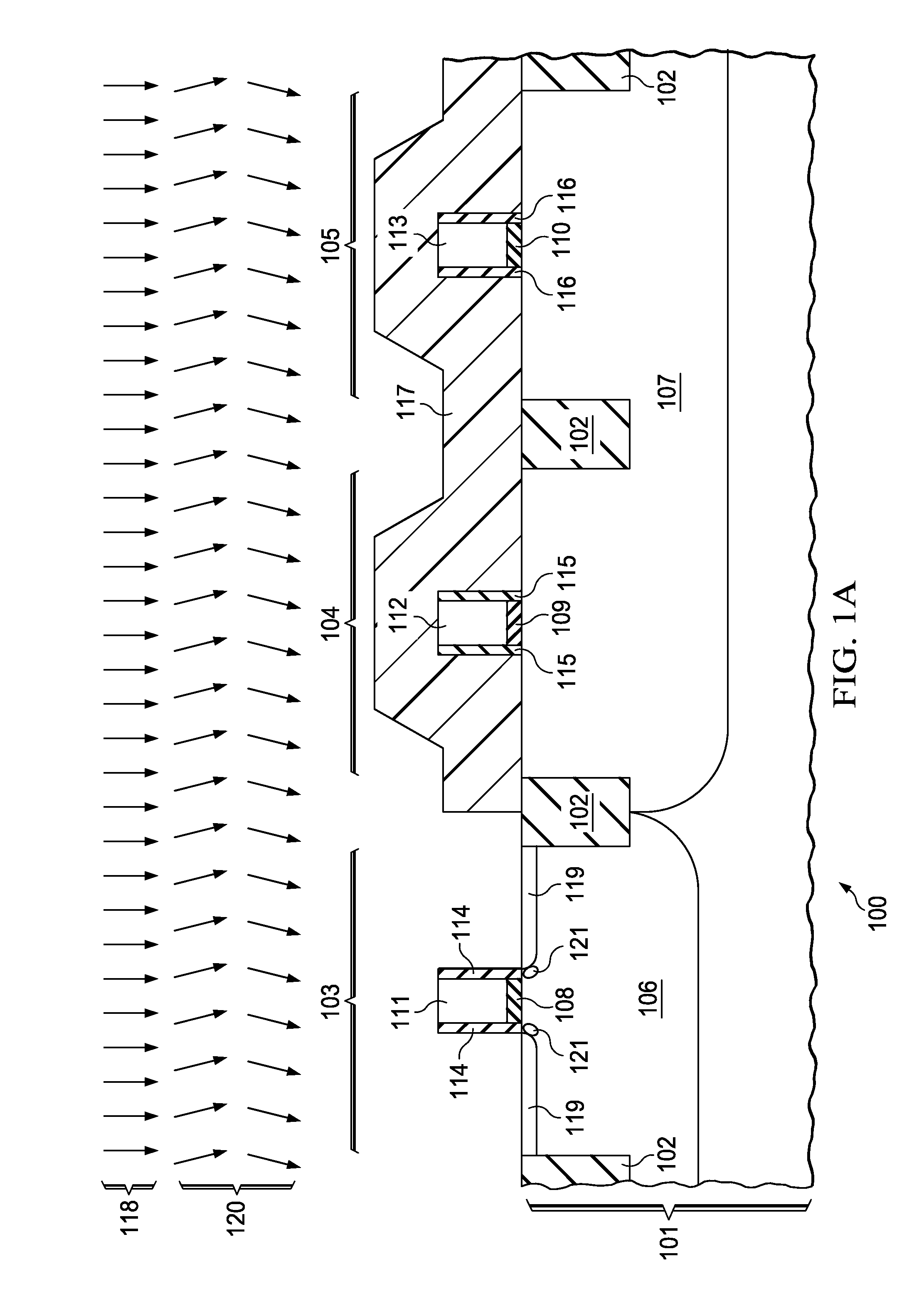
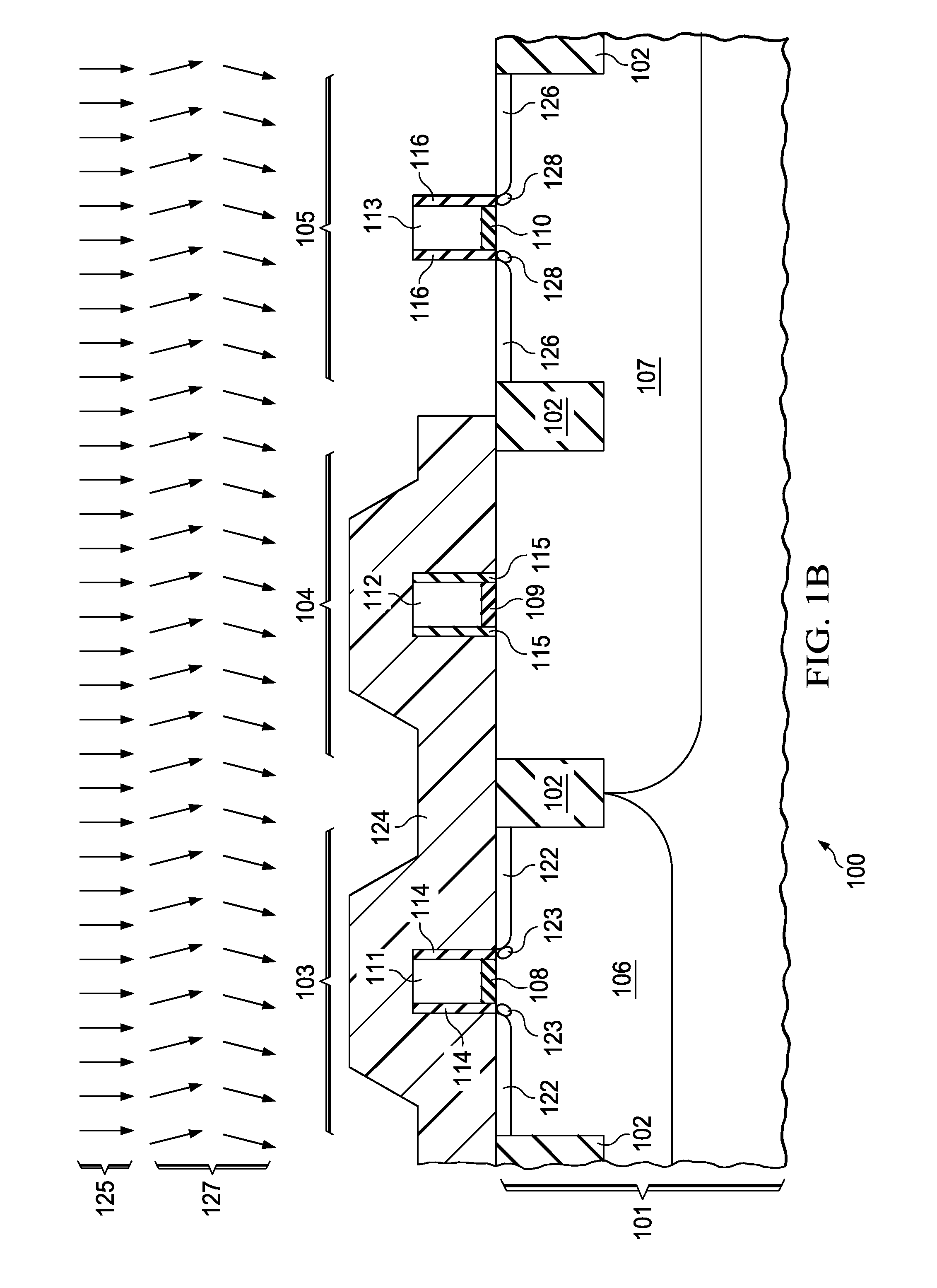
[0019]FIG. 1A through FIG. 1D are cross-sections of a CMOS IC including a gated quantum well device formed according to the instant invention, depicted in successive stages of fabrication. Referring to FIG. 1A, the IC (100) is formed in a semiconductor substrate (101), typically p-type single crystal silicon, but possibly a silicon-on-insulator (SOI) substrate, a hybrid orientation technology (HOT) substrate with regions of silicon or silicon-germanium with different crystal orientations, or any other structure appropriate for fabrication of a CMOS IC. Elements of field oxide (102) are formed by a shallow trench isolation (STI) process sequence, in which trenches, commonly 200 to 500 nanometers deep, are etched into the substrate (101), electrically passivated, commonly by growing a thermal oxide layer on sidewalls of the trenches, and filled with insulating material, typically silicon dioxide, commonly by a high density plasma (HDP) process or an ozone based thermal chemical vapor ...
second embodiment
[0036]FIG. 5A through FIG. 5C are cross-sections of a CMOS IC including a gated quantum well device formed according to the instant invention, depicted in successive stages of fabrication. Referring to FIG. 5A, the IC (500) is formed in a semiconductor substrate (501) with the properties described in reference to FIG. 1A. Elements of field oxide (502) are formed in the substrate (501) by an STI process, separating an NMOS region (503), a gated quantum well device region (504) and a PMOS region (505). A p-well (506) is formed in the substrate (501) in the NMOS region (503) and the gated quantum well device region (504) as described in reference to FIG. 1A. Similarly, an n-well (507) is formed in the substrate (501) in the PMOS region (505) as described in reference to FIG. 1A. An NMOS gate dielectric layer (508), a gated quantum well device gate dielectric layer (509) and a PMOS gate dielectric layer (510) are formed on top surfaces of the substrate (501), with the properties describ...
PUM
 Abstract
Description
Claims
Application Information
 - R&D
- Intellectual Property
- Life Sciences
- Materials
- Tech Scout
- Unparalleled Data Quality
- Higher Quality Content
- 60% Fewer Hallucinations
Browse by: Latest US Patents, China's latest patents, Technical Efficacy Thesaurus, Application Domain, Technology Topic, Popular Technical Reports.
© 2025 PatSnap. All rights reserved.Legal|Privacy policy|Modern Slavery Act Transparency Statement|Sitemap|About US| Contact US: help@patsnap.com


