
Solution-processed high mobility inorganic thin-film transistors

a technology of inorganic and thin-film transistors, which is applied in the direction of semiconductor devices, electrical equipment, basic electric elements, etc., can solve the problems of limiting the temperature at which the semiconductor film is deposited, the annealing temperature is incompatible with inexpensive plastic substrates, and the solution-processed high-speed circuit is deposited. achieve enhanced texturing, improve surface morphology, and enhance the effect of properties

Inactive Publication Date: 2011-09-13
NORTHWESTERN UNIV
View PDF20 Cites 62 Cited by
  • Summary
  • Abstract
  • Description
  • Claims
  • Application Information

AI Technical Summary

Benefits of technology

[0009]It can be an object of the present invention to provide material components, structures and / or device configurations meeting the aforementioned requirements while, in addition, fully realizing the benefits available from TFT technologies.
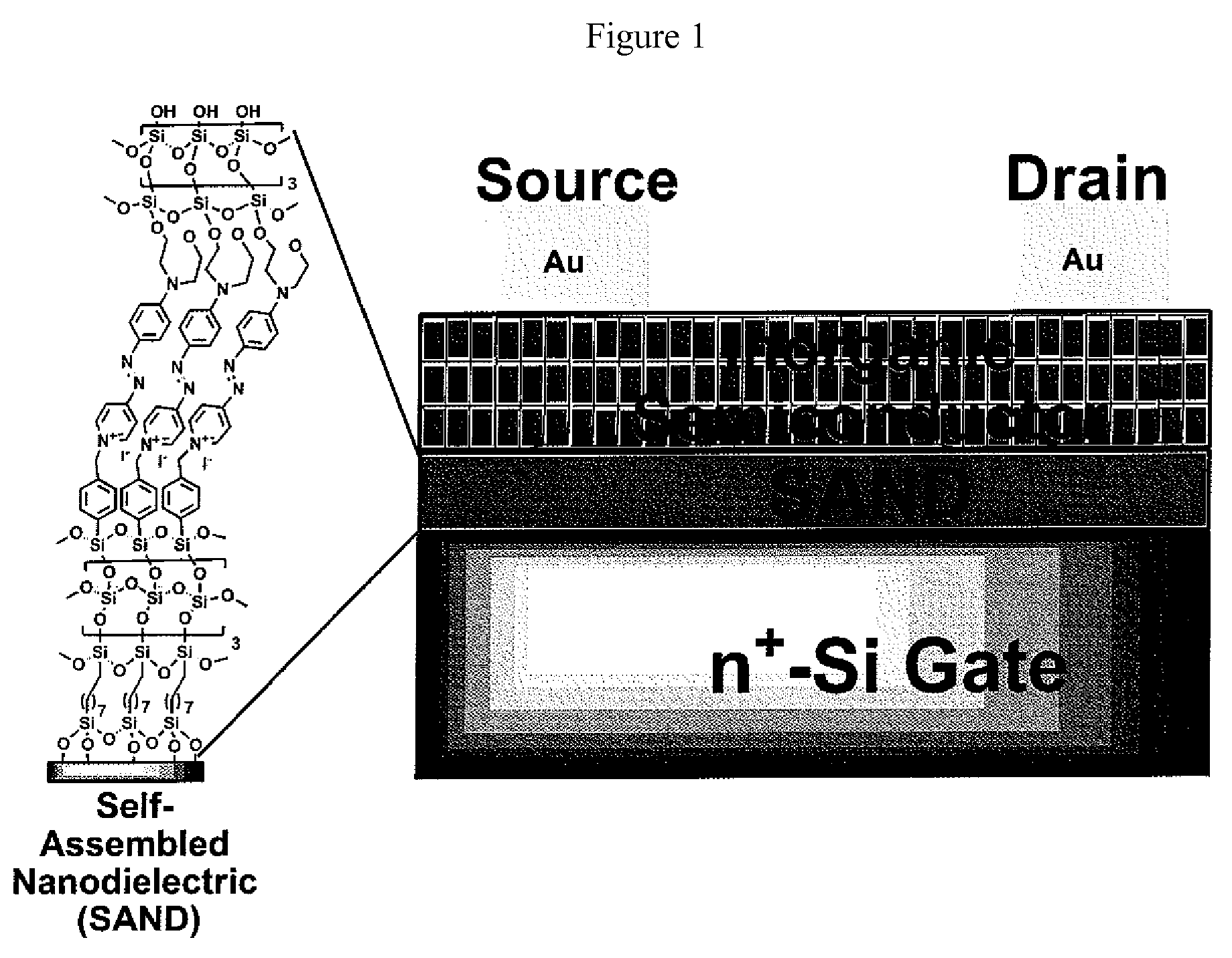
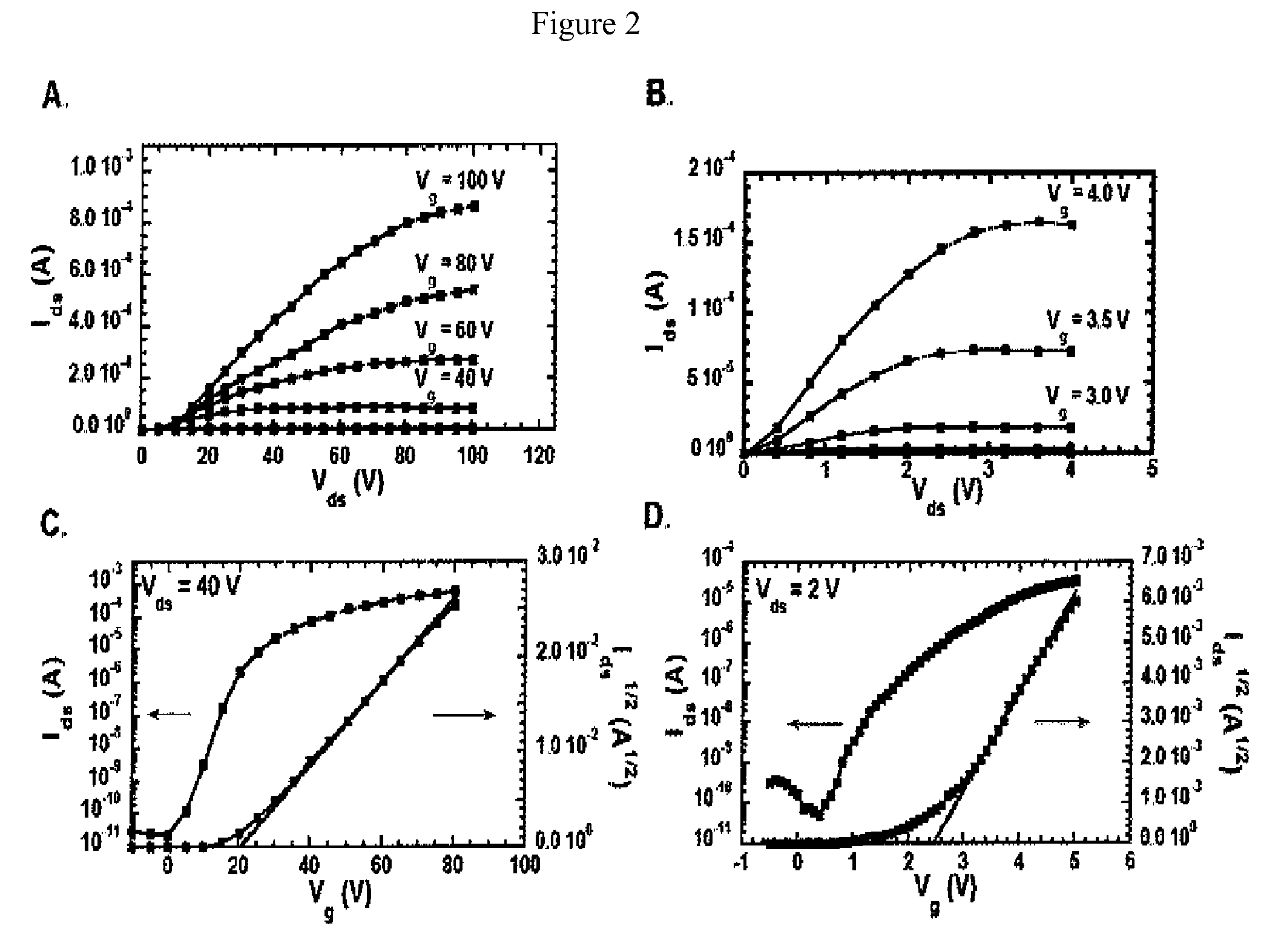
[0047]In certain embodiments, the present teachings can relate to high-performance inorganic-organic hybrid TFTs fabricated, for example, with solution-processed polycrystalline metal oxide semiconducting thin-films (e.g., In2O3) as the channel material and a range of thin organic dielectrics. In other embodiments, the present teachings can relate to TFTs incorporating inorganic dielectrics such as but not limited to SiO2. As shown below, it was found that inorganic crystalline semiconductor components with sufficient microstructural crystallinity can exhibit n-type field-effect behavior, and thin organic (or inorganic) dielectric components with sufficient insulating properties can enable ultra-low-voltage TFT operation. Such hybrid TFTs can show exceptionally large field-effect mobilities of >40 cm2 / V s at low operating voltages (1˜2 V).

Problems solved by technology

These observations suggest that conventional OTFTs will be useful for low- or medium-performance applications but not for solution-processed high-speed circuits.
However, inorganic semiconductors are typically intractable in common solvents so that soluble precursors must be employed, then converted to the active semiconducting films.
High annealing temperatures are incompatible with inexpensive plastic substrates.
Thus, these requirements significantly limit the temperatures at which the semiconductor films can be annealed and / or the choice of materials for the gate dielectric.
For example, ultra-thin inorganic films deposited from solution are invariably leaky and morphologically very rough.
Meanwhile, many known polymeric dielectric materials are not sufficiently stable, whether thermally and / or mechanically, to withstand high annealing temperatures and aggressive aqueous solutions.
As such, to date, TFTs have not been fabricated using both a solution-processed inorganic semiconductor and a solution-processed gate dielectric.
Their films inevitably suffer from problems associated with large densities of grain boundaries, including instability to air due to O2 / H2O / CO2 chemisorption and film surface roughness due to facet formation.
However, in these studies, the different vapor pressures of the individual element precursors often lead to difficulties in tuning the optimum film composition and, importantly, reproducibility problems.
In addition, low-pressure deposition processes are expensive to scale for large areas and high throughput.
Meanwhile, previous metal-oxide-based TFTs fabricated by solution deposition generally exhibit poor performance, in particular low field-effect mobilities, low Ion:Ioff ratios and large operating voltages, any of which tend to preclude most practical applications.

Method used


Image

  • Solution-processed high mobility inorganic thin-film transistors
  • Solution-processed high mobility inorganic thin-film transistors
  • Solution-processed high mobility inorganic thin-film transistors

Examples


example 1a

CdSe Film Deposition

[0085]The reagents CdCl2, Se, and Na2SO3 were purchased from Aldrich Chemicals and were used without further purification. The aqueous ammonia (28-30%) solution was purchased from Mallinckrodt Baker. The water used in all the deposition steps was purified with a Millipore nanopure water system. The Na2SeSO3 solution was prepared from 0.37 g (4.7 mmol) of Se in 40 mL of a 0.2 M (7.9 mmol) Na2SO3 solution which was heated at 60° C. for 1.5 h in a water bath to from the Na2SeSO3. The undissolved Se was then removed by filtration with filter paper and resulting filtrate used in the CBD solution. The CBD solution was prepared from 20 mL of ˜0.1 M aqueous CdCl2, 6.0 ml concentrated NH4OH, and 20 mL of ˜0.1 M aqueous Na2SeSO3 solution. This solution was then heated to 80° C. using a water bath. After the solution became orange, the substrates (7×2.5 cm) loaded into a glass holder and were immersed in the CBD solution. The substrates were initially placed in the solution...

example 1b

[0086]For patterning of the semiconductor film growth, solutions of the polystyrene (Mw=250 K) and polymethyl methacrylate (350 K) were brushed onto the substrates to define deposition regions on the Si substrate. The concentration of the polymer solutions was 100 mg / mL in toluene and TFT for polystyrene and polymethyl methacrylate, respectively. After 20 min of air drying, the patterned substrates were heated (65° C.) under vacuum for 1 h. CBD of the CdSe was then performed. Following the nanopure water washings, the CdSe coated substrates were sonicated three times in 50 mL of THF for 5 min and subsequently washed twice in nanopure water for 5 min. This procedure results in ˜12 mm2 patterned CdSe films.

example 2

Zinc Indium Oxide Film Deposition

[0087]A 0.1 M solution of zinc acetate (Zn(OAC)2) in 2-methoxy-ethanol was prepared. The compound 2-amino-ethanol was added to the solution in a 1:1 ratio with the Zn(OAC)2 to increase the Zn(OAC)2 solubility to afford a solution concentration of 0.1 M. A 0.1 M solution of InCl3 in was also prepared 2-methoxy-ethanol. The spin-casting solution was prepared by mixing 0.5 ml of the InCl3 solution and 0.5 ml of the Zn(OAC)2 solution. The precursor film was then spun cast at 1500 rpm. The precursor film was then pre-annealed at 180° C. for 10 min and then a second coat of ZIO was spun-cast and pre-annealed the ZIO film was then annealed at 400° C. for 30 min.


PUM

PropertyMeasurementUnit
temperatureaaaaaaaaaa

Abstract

Fluid media comprising inorganic semiconductor components for fabrication of thin film transistor devices.

Description

CROSS REFERENCE TO RELATED APPLICATIONS[0001]This application claims priority to and the benefit of U.S. Provisional Patent Application Ser. Nos. 61 / 063,089, filed on Jan. 31, 2008, and 61 / 189,351, filed on Aug. 18, 2008, the disclosure of each of which is incorporated by reference herein in its entirety.STATEMENT REGARDING FEDERALLY SPONSORED RESEARCH OR DEVELOPMENT[0002]This invention was made with government support under Grant Nos. STTR TSI-2260-0674731 / W31P4Q-05-C-0335 awarded by the U.S. Army Aviation and Missile Command. The government has certain rights in the invention.BACKGROUND OF THE INVENTION[0003]The fabrication of high-performance thin-film transistors (TFTs) by solution phase processes is a promising approach to developing commercially viable, low-cost, large-area electronics. Despite intense efforts to develop solution-processed organic semiconducting films, the highest field-effect mobilities (μFETs) for organic TFTs (OTFTs) reported to date are ˜1.0 cm2 V−1 s−1 (p...

Claims


Application Information

Patent Timeline
Patent Type & Authority Patents(United States)
IPC IPC(8): H01L21/00
CPCH01L21/02554H01L21/0256H01L21/02565H01L27/1292H01L29/78681H01L29/7869H01L21/02628H01L21/208
Inventor MARKS, TOBIN J.FACCHETTI, ANTONIOBYRNE, PAUL D.KIM, HYUN SUNG
Owner NORTHWESTERN UNIV
Learn More