
Optimal timing-driven cloning under linear delay model

a linear delay and timing-driven technology, applied in the field of semiconductor chip and integrated circuit design, can solve the problems of large number of cells, difficult physical design without the aid of computers, and complicated connections between cells,

Active Publication Date: 2011-09-06
SIEMENS PROD LIFECYCLE MANAGEMENT SOFTWARE INC
View PDF8 Cites 1 Cited by
  • Summary
  • Abstract
  • Description
  • Claims
  • Application Information

AI Technical Summary

Benefits of technology

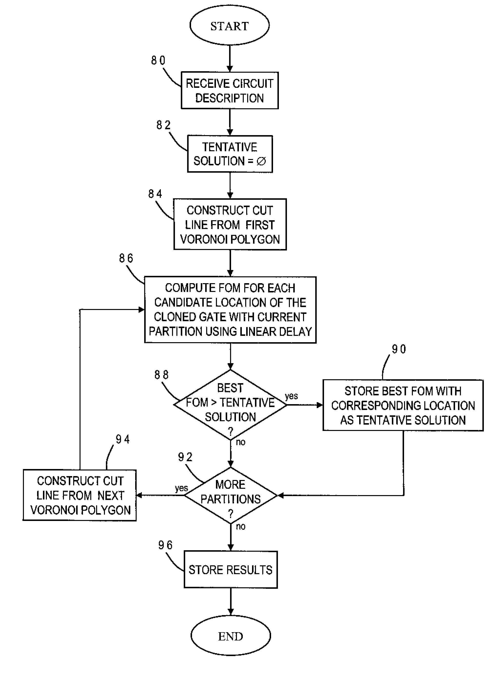
The present invention provides an improved cloning method for designing the layout of an integrated circuit that is timing-driven. This method can be used with interconnect modeling and buffering, and is computationally efficient. The method involves iteratively partitioning the sinks of the original gate into different sets of clusters, and computing a figure of merit for each location of the cloned gate to optimize timing based on delay. The best solution is selected based on the highest figure of merit, and the location of the original gate may also be changed to a new location that optimizes timing based on delay. The sinks are advantageously partitioned using boundaries of Voronoi polygons or the diamond region surrounding the original gate. The technical effects of this invention include improved efficiency and accuracy in designing integrated circuits.

Problems solved by technology

An IC may include a very large number of cells and require complicated connections between the cells.
Due to the large number of components and the details required by the fabrication process for very large scale integrated (VLSI) devices, physical design is not practical without the aid of computers.
However, physical synthesis can take days to complete, and the computational requirements are increasing as designs are ever larger and more gates need to be placed.
There are also more chances for bad placements due to limited area resources.
As process technology scales to the submicron regime, interconnect delays increasingly dominate gate delays.
Timing closure is an important problem for ASIC and server designs with 90 nm technology and beyond.
While cloning is useful for solving some timing problems, it is not particularly efficient.
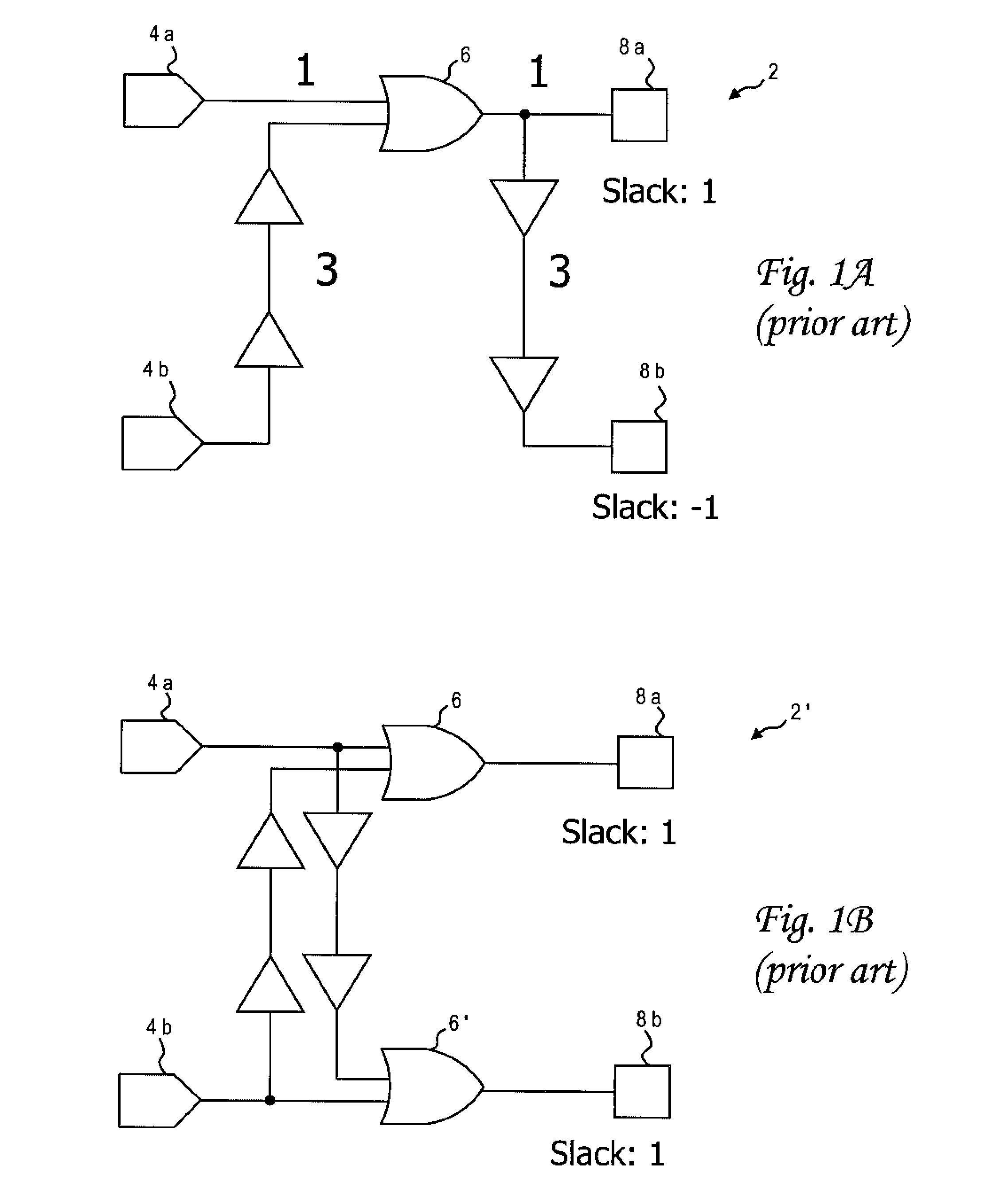
Prior art cloning uses gate delay models (the delay through a gate is proportional to the total capacitances of gates which it drives), ignoring the interconnect delay and physical layout information, and does not determine an optimum location of the duplicated gate.
For example, if the cloned gate 6′ in FIG. 1B had been placed too near the original gate 6, the net would still exhibit poor slack.
Existing cloning techniques have difficulty even determining a good partition where there are many sinks in the net.

Method used


Image

  • Optimal timing-driven cloning under linear delay model
  • Optimal timing-driven cloning under linear delay model
  • Optimal timing-driven cloning under linear delay model

Examples


Embodiment Construction

)

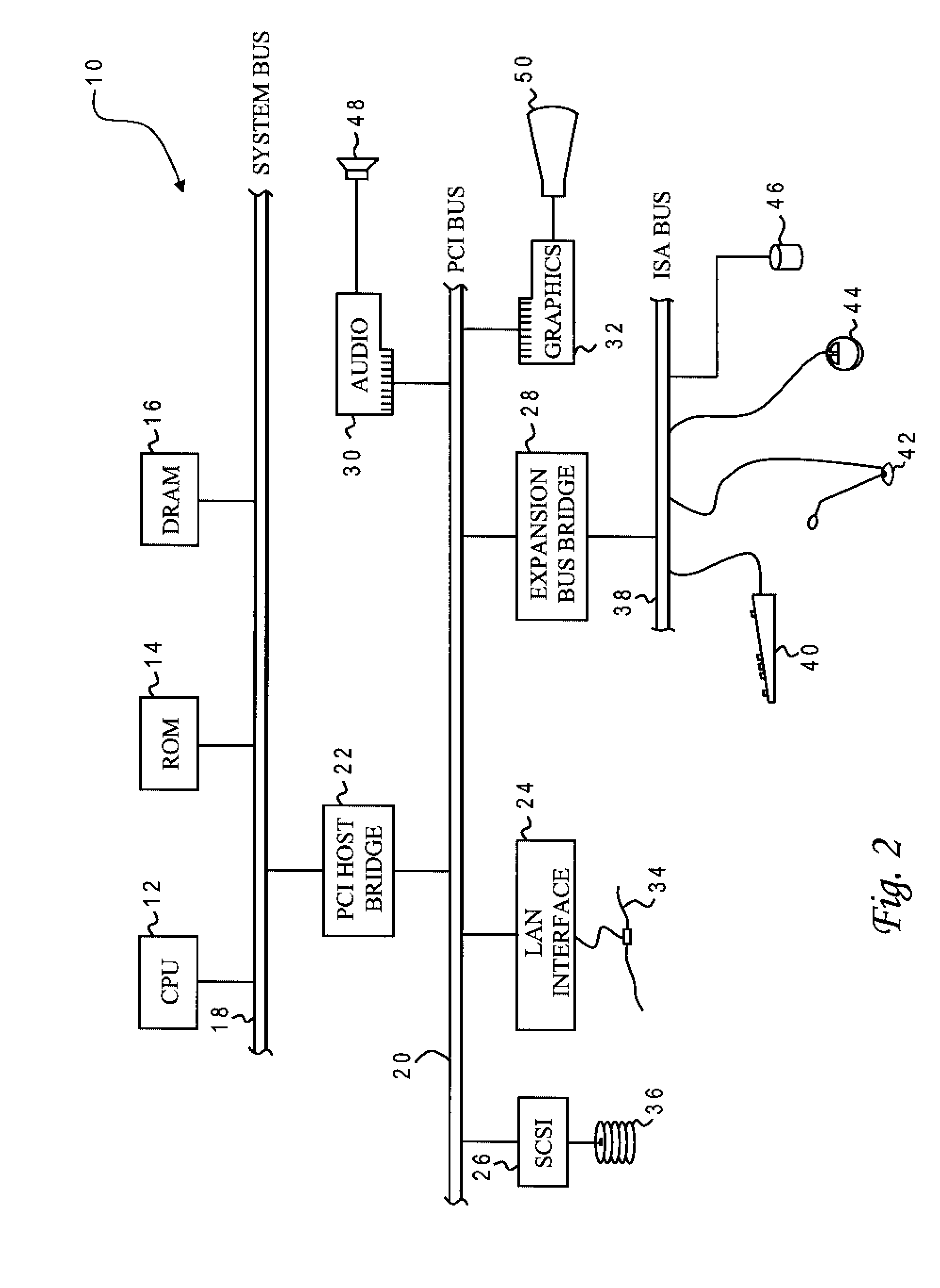
[0023]With reference now to the figures, and in particular with reference to FIG. 2, there is depicted one embodiment 10 of a computer system programmed to carry out timing-driven cloning in accordance with one implementation of the present invention. System 10 includes a central processing unit (CPU) 12 which carries out program instructions, firmware or read-only memory (ROM) 14 which stores the system's basic input / output logic, and a dynamic random access memory (DRAM) 16 which temporarily stores program instructions and operand data used by CPU 12. CPU 12, ROM 14 and DRAM 16 are all connected to a system bus 18. There may be additional structures in the memory hierarchy which are not depicted, such as on-board (L1) and second-level (L2) caches. In high performance implementations, system 10 may include multiple CPUs and a distributed system memory.

[0024]CPU 12, ROM 14 and DRAM 16 are coupled to a peripheral component interconnect (PCI) local bus 20 using a PCI host bridge 22. ...


PUM


Abstract

A timing-driven cloning method iteratively partitions sinks of the net into different sets of clusters and for each set computes a figure of merit for a cloned gate location which optimizes timing based on linear delay, that is, a delay proportional to the distance between the cloned gate location and the sinks. The set having the highest figure of merit is selected as the best solution. The original gate may also be moved to a timing-optimized location. The sinks are advantageously partitioned using boundaries of Voronoi polygons defined by a diamond region surrounding the original gate, or vice versa. The figure of merit may be for example worst slack, a sum of slacks at the sinks in the second cluster, or a linear combination of worst slack and sum of the slacks.

Description

BACKGROUND OF THE INVENTION[0001]1. Field of the Invention[0002]The present invention generally relates to the design of semiconductor chips and integrated circuits, and more particularly to the use of cloning techniques to manage timing requirements in an integrated circuit design.[0003]2. Description of the Related Art[0004]Integrated circuits are used for a wide variety of electronic applications, from simple devices such as wristwatches, to the most complex computer systems. A microelectronic integrated circuit (IC) chip can generally be thought of as a collection of logic cells with electrical interconnections between the cells, formed on a semiconductor substrate (e.g., silicon). An IC may include a very large number of cells and require complicated connections between the cells. A cell is a group of one or more circuit elements such as transistors, capacitors, resistors, inductors, and other basic circuit elements grouped to perform a logic function. Cell types include, for e...

Claims


Application Information

Patent Timeline
Patent Type & Authority Patents(United States)
IPC IPC(8): G06F17/50
CPCG06F17/5031G06F30/3312
Inventor ALPERT, CHARLES J.LI, ZHUOPAPA, DAVID A.SZE, CHIN NGAI
Owner SIEMENS PROD LIFECYCLE MANAGEMENT SOFTWARE INC
Learn More