High frequency power detector circuit and radio communication device

a detector circuit and high frequency technology, applied in the field of detector circuits, can solve problems such as detection error and detection power level error, and achieve the effect of increasing the circuit dimension

Active Publication Date: 2011-08-09
PANASONIC CORP
View PDF11 Cites 6 Cited by
  • Summary
  • Abstract
  • Description
  • Claims
  • Application Information

AI Technical Summary

Benefits of technology

[0015]With the foregoing in mind, an object of the present invention is to provide a high frequency power detector circuit which reduces the detection error caused by variations in the course of manufacture, change in temperature and change in supply voltage and reduces the area of the circuit, and a radio communication device including the circuit.
[0017]According to the configuration, an envelope of the high frequency signal is detected by the first envelope detector circuit, a reference voltage for power level detection is generated by the second envelope detector circuit of the same structure as the first envelope detector circuit and an output of the first envelope detector circuit is detected by the detector with reference to an output of the second envelope detector circuit. As a result, the power level of the input high frequency signal is detected. The first and second envelope detector circuits may be provided without using a current source. Further, there is no need of additionally providing a reference voltage generating circuit. Accordingly, the total number of resistance elements is kept small. Therefore, as compared with conventional ones, the high frequency power detector circuit is improved in resistance against variations in the course of manufacture, change in temperature and change in supply voltage, thereby raising precision of high frequency power detection, and is reduced in size.

Problems solved by technology

Therefore, an absolute resistance value varies due to variations in the course of manufacture, change in temperature and change in supply voltage, thereby causing an error in detected power level.
However, an error in detected power level may occur due to an error in input reference current and a mismatch between threshold values of paired transistors in the current mirror circuit.

Method used


Image

  • High frequency power detector circuit and radio communication device
  • High frequency power detector circuit and radio communication device
  • High frequency power detector circuit and radio communication device

Examples


embodiment 1

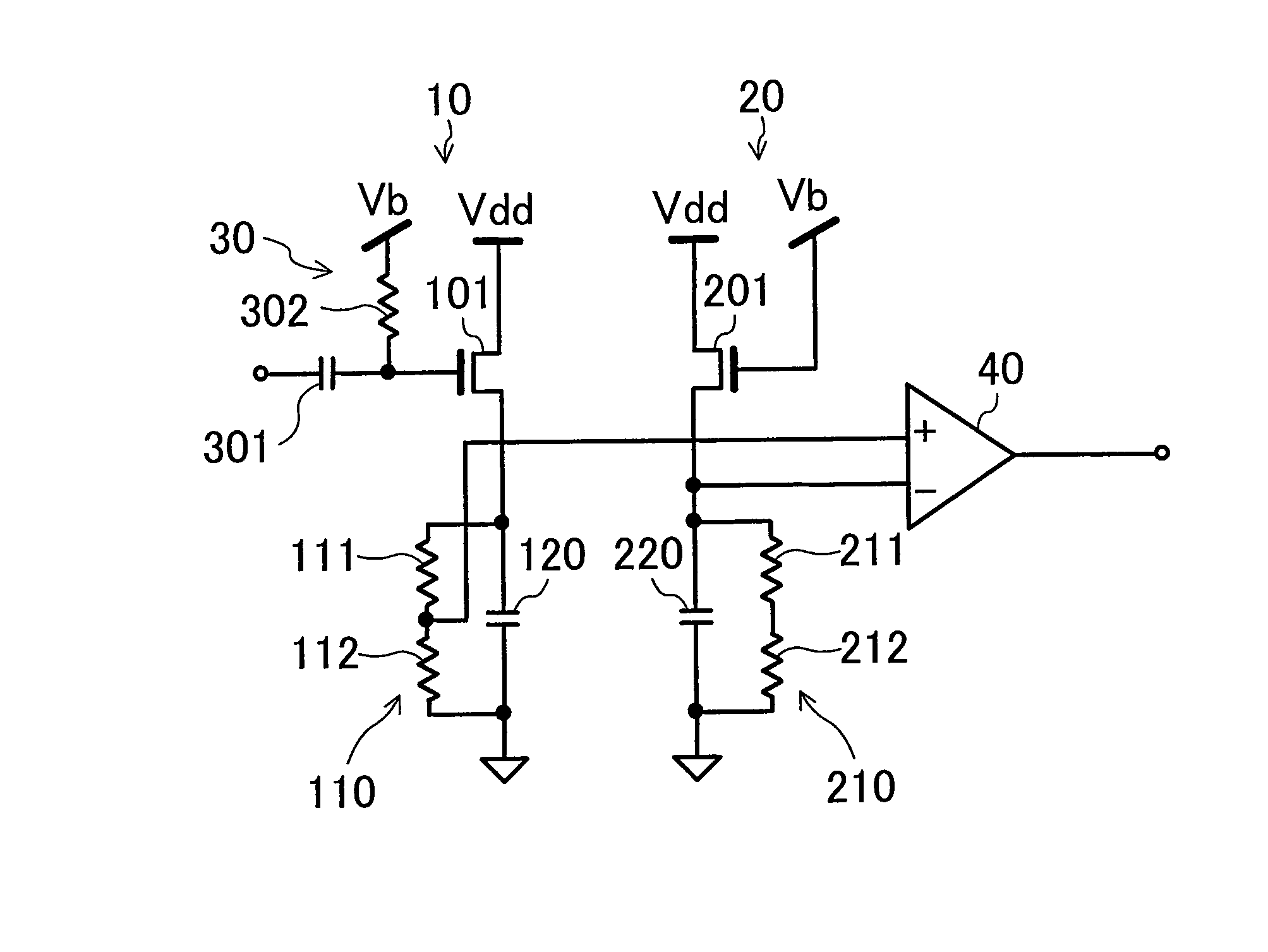
[0027]FIG. 1 shows the structure of a high frequency power detector circuit according to Embodiment 1. The high frequency power detector circuit of the present embodiment includes two envelope detector circuits 10 and 20, a level shifter 30 and a detector 40. In the envelope detector circuit 10, a drain of an N-channel field effect transistor 101 is connected to a supply voltage Vdd and a resistance row 110 including two serially-connected resistance elements 111 and 112 and a capacitative element 120 are connected to a source the transistor 101 in parallel. The structure of another envelope detector circuit 20 is the same as that of the envelope detector circuit 10. That is, in the envelope detector circuit 20, a drain of an N-channel field effect transistor 201 is connected to a supply voltage Vdd and a resistance row 210 including two serially-connected resistance elements 211 and 212 and a capacitative element 220 are connected to a source of the transistor 201 in parallel. In t...

embodiment 2

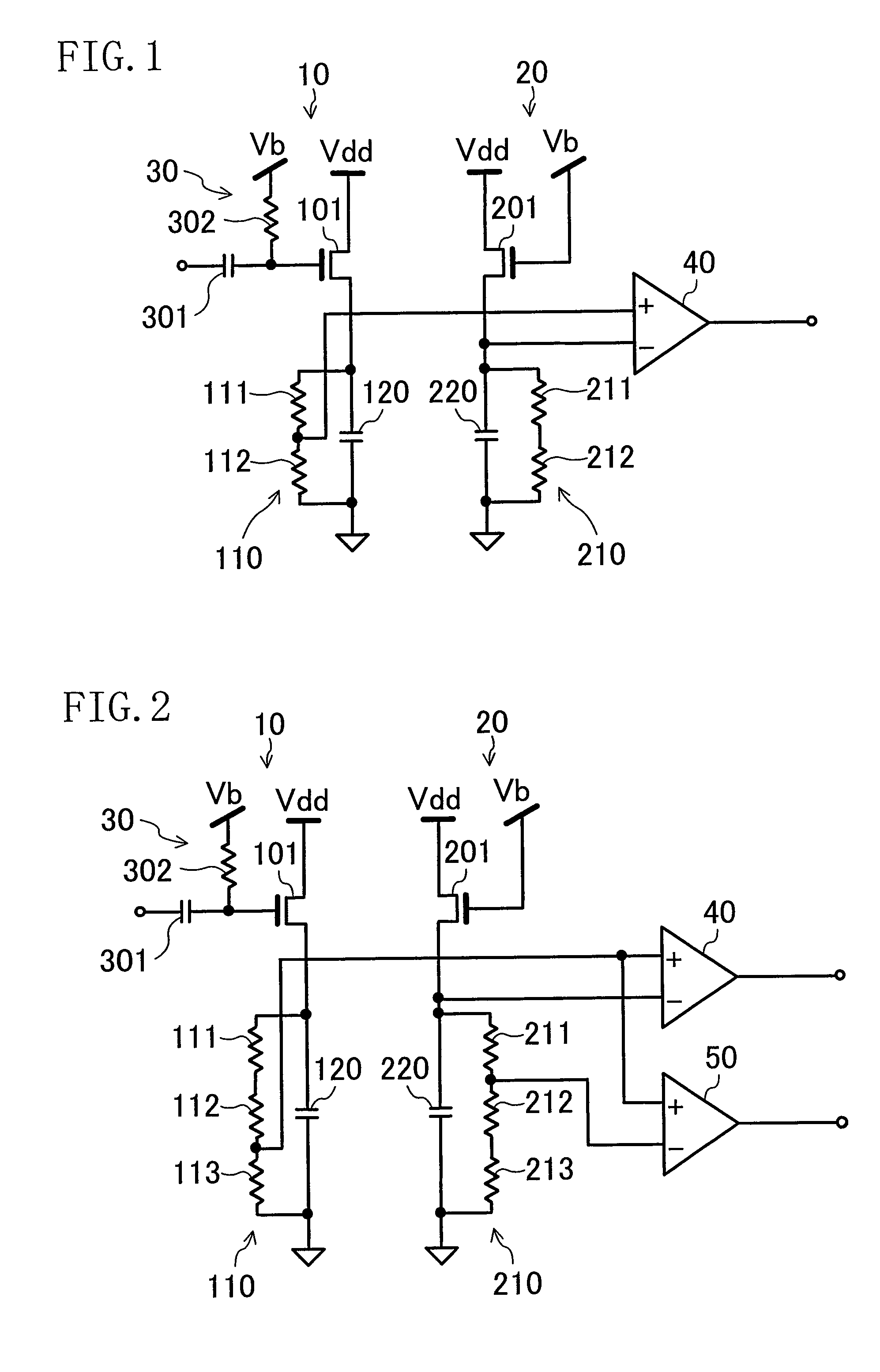
[0036]FIG. 2 shows the structure of a high frequency power detector circuit according to Embodiment 2. In an automatic gain control system of a common receiver, a feed back control system performs hysteresis control to ensure stability. For this reason, an upper limit and a lower limit of the power level of a high frequency signal have to be detected. According to the high frequency power detector circuit of the present embodiment, the power level of an input high frequency signal can be detected based on two reference voltages. More specifically, the high frequency power detector circuit of the present embodiment is the same as the high frequency power detector circuit of Embodiment 1 except that a detector 50 is additionally provided. The difference from the structure of Embodiment 1 is described below in detail.

[0037]In an envelope detector circuit 10, a resistance row 110 includes three resistance elements 111, 112 and 113 connected in series. Among intermediate terminal voltage...

embodiment 3

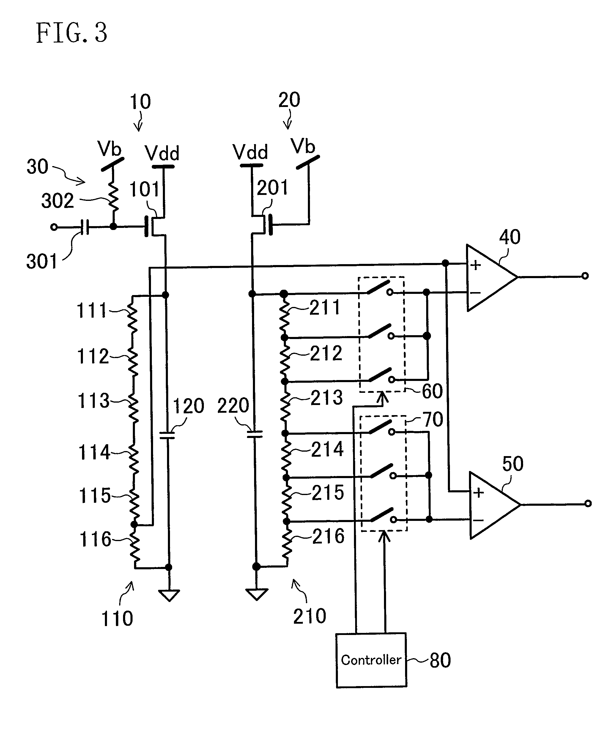
[0040]FIG. 3 shows the structure of a high frequency power detector circuit according to Embodiment 3. The high frequency power detector circuit of the present embodiment is the same as the high frequency power detector circuit of Embodiment 2 except that selectors 60 and 70 for switching between the first and second reference voltages output from the envelope detector circuit 20 and a controller 80 are additionally provided. The difference from Embodiment 2 is described below in detail.

[0041]In an envelope detector circuit 10, a resistance row 110 includes six resistance elements 111, 112, 113, 114, 115 and 116 connected in series. Among intermediate terminal voltages of the resistance row 110, the envelope detector circuit 10 outputs the one which is the nearest to a ground node, i.e., a voltage at a connection point between the resistance elements 115 and 116. In an envelope detector circuit 20, a resistance row 210 includes six resistance elements 211, 212, 213, 214, 215 and 216...


PUM


Abstract

First and second envelope detector circuits have, respectively, a resistance row, a capacitative element connected to the resistance row in parallel and a transistor connected between a connection point between the resistance row and the capacitative element and a predetermined voltage node. An output of a level shifter is supplied to a gate or a base of the transistor of the first envelope detector circuit. A predetermined voltage is supplied to a gate or a base of the transistor of the second envelope detector circuit. A detector detects an intermediate terminal voltage of the resistance row of the first envelope detector circuit with reference to a total voltage or an intermediate terminal voltage of the resistance row of the second envelope detector circuit.

Description

CROSS-REFERENCE TO RELATED APPLICATION[0001]This non-provisional application claims priority under 35 U.S.C. §119(a) of Japanese Patent Application No. 2007-276417 filed in Japan on Oct. 24, 2007, the entire contents of which are hereby incorporated by reference.BACKGROUND OF THE INVENTION[0002]1. Field of the Invention[0003]The present invention relates to a detector circuit for detecting high frequency signal power. In particular, it relates to a high frequency power detector circuit useful for automatic gain control and automatic power level control in radio communication devices.[0004]2. Description of Related Art[0005]In recent years, cellular phone terminals have been provided with various radio communication functions such as digital television, FM radio, Bluetooth® and wireless LAN in addition to a telephone function. In order to meet increasing demand for reduction in size and cost of radio communication terminals and modules included in them, integration of high performanc...

Claims


Application Information

Patent Timeline
Patent Type & Authority Patents(United States)
IPC IPC(8): H04B1/04H04B1/3822H04B1/40
CPCH03G3/3052G01R21/12
Inventor KIM, RYANGSUKIMURA, HIROSHI
Owner PANASONIC CORP
Why Eureka
Try Eureka