Silicon-based thin-film photoelectric converter and method of manufacturing the same
a technology of thin-film photoelectric converters and silicon-based thin-film photoelectric converters, which is applied in the manufacture of final products, basic electric elements, coatings, etc., can solve the problem that amorphous silicon cannot be used for a photoelectric converter such as amorphous silicon, and achieve the effects of reducing contact resistance at the interface, high hydrogen concentration, and resistivity reduction
- Summary
- Abstract
- Description
- Claims
- Application Information
AI Technical Summary
Benefits of technology
Problems solved by technology
Method used
Image
Examples
example 1
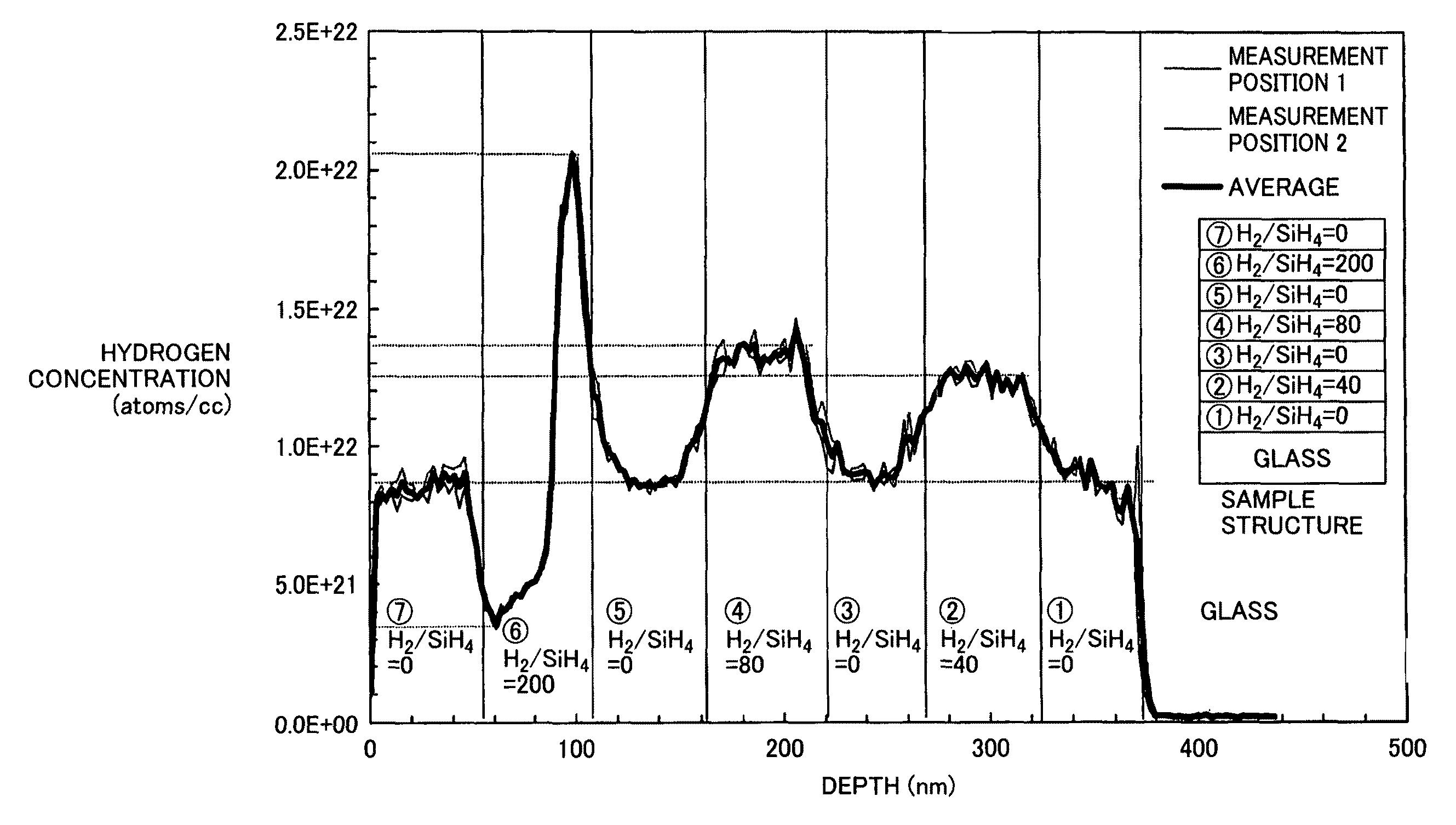
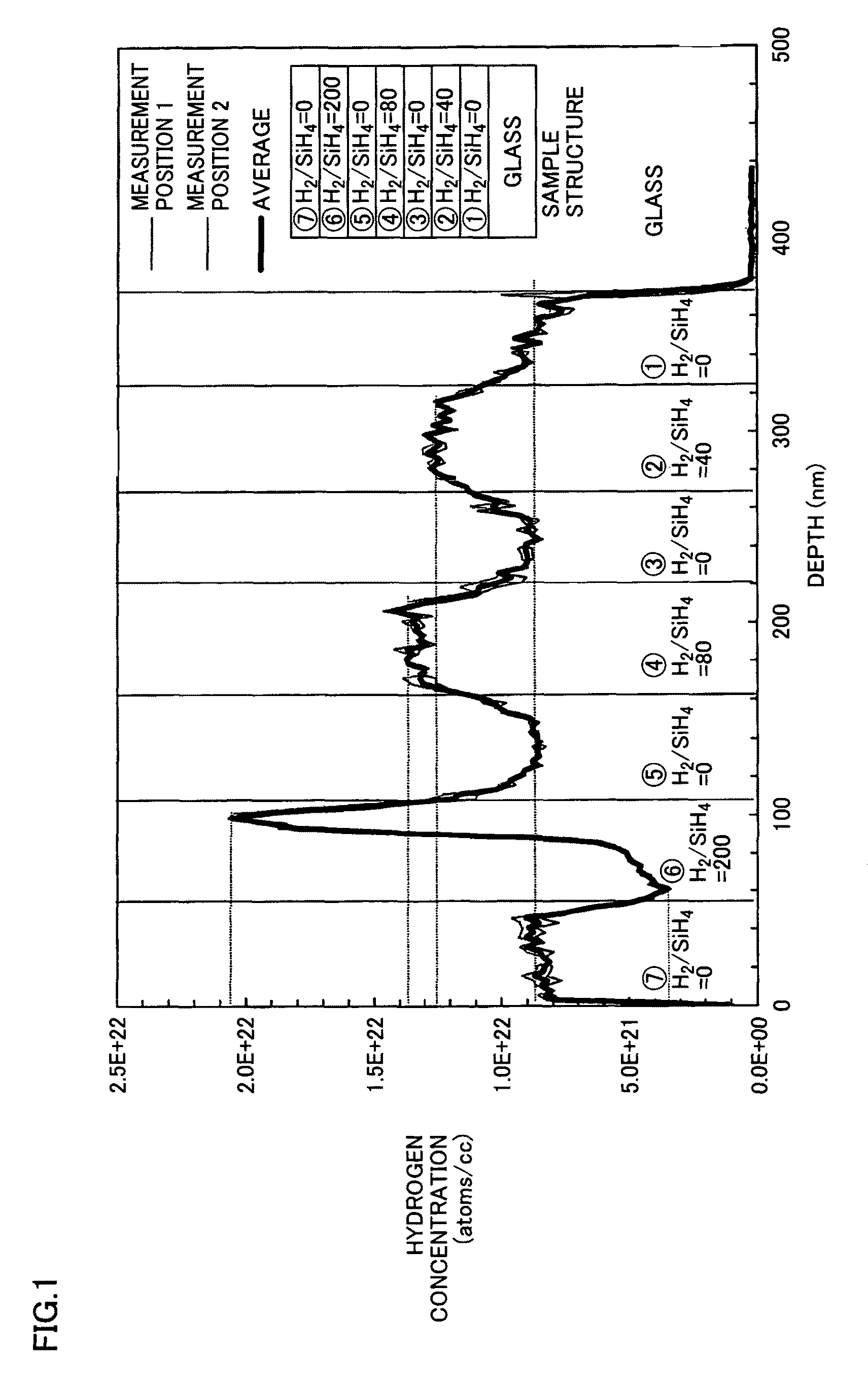
[0083]A single-junction amorphous photoelectric converter as shown in FIG. 4 was formed as Example 1. The device of Example 1 as shown in FIG. 4 differs from that of Comparative Example 2 in that substantially i-type buffer layer 33 mainly made of hydrogenated amorphous silicon was used instead of n-type microcrystalline silicon layer 37 in FIG. 7. Buffer layer 33 had a thickness of 5 nm. The deposition conditions for buffer layer 33 were as follows: chamber P5 serving as an n-type film-deposition chamber was used under conditions of an H2 / SiH4 flow ratio=80, a gas flow rate of H2 / SiH4=12800 / 160 sccm, a power supply frequency of 13.56 MHz, a power density of 100 mW / cm2, a pressure of 600 Pa, and a substrate temperature of 200° C. Hydrogen concentration at the buffer layer's interface with the photoelectric conversion layer was 1.37×10²² atoms / cc, when measured by SIMS. Hydrogen concentration of the photoelectric conversion layer was 8.5×10²¹ atoms / cc. In this case, tact time in cham...
example 2
[0086]A photoelectric converter having a structure similar to that of Example 1 was formed in Example 2, which was different from Example 1 only in that buffer layer 33 was deposited in chamber P4 serving as an i-type film-deposition chamber. Photoelectric conversion layer 32 was deposited in chamber P2, chamber P3, and chamber P4, and then buffer layer 33 was deposited within the remaining time allowed for chamber P4 and tact time in chamber P4 was 10 minutes. Furthermore, n-type Si1-xOx layer 34 and n-type microcrystalline silicon layer 35 were deposited in chamber P5, and tact time in chamber P5 was 11 minutes. Therefore, either of chambers P4 and P5 does not cause a rate-limiting factor in the manufacturing tact time, and hence manufacturing tact time in the CVD apparatus was 12 minutes, which was the same as that in Comparative Example 1.
[0087]As shown in Table 1, output properties of the photoelectric converter in Example 2 were as follows: Voc=0.883 V, Jsc=14.37 mA / cm2, FF=0....
example 3
[0088]Photoelectric converters of Example 3 were formed with a similar structure and formation method as for the amorphous photoelectric converter of Example 1, except only that the thickness of buffer layer 33 was varied. At that time, the H2 / SiH4 for depositing the buffer layer was set to be 80. FIGS. 8-11 show correlation diagrams of various output properties of the photoelectric converters of Example 3 with respect to thickness of the buffer layer, by using relative values with respect to the output properties of the photoelectric converter of Comparative Example 2.
[0089]FIG. 8 is a correlation diagram that shows a relationship between thickness of the buffer layer and conversion efficiency (Eff) of the photoelectric converter in Example 3. As thickness of the buffer layer increases, Eff drastically increases to reach the maximum value at a thickness of 10-20 nm and then gradually decreases. The Eff becomes higher in the buffer layer's thickness range of 5 nm to 50 nm, as compar...
PUM
| Property | Measurement | Unit |
|---|---|---|
| thickness | aaaaa | aaaaa |
| thickness | aaaaa | aaaaa |
| thickness | aaaaa | aaaaa |
Abstract
Description
Claims
Application Information
 - R&D
- Intellectual Property
- Life Sciences
- Materials
- Tech Scout
- Unparalleled Data Quality
- Higher Quality Content
- 60% Fewer Hallucinations
Browse by: Latest US Patents, China's latest patents, Technical Efficacy Thesaurus, Application Domain, Technology Topic, Popular Technical Reports.
© 2025 PatSnap. All rights reserved.Legal|Privacy policy|Modern Slavery Act Transparency Statement|Sitemap|About US| Contact US: help@patsnap.com


