Semiconductor device and method of manufacturing the same

a semiconductor and surface layer technology, applied in semiconductor devices, semiconductor/solid-state device details, electrical apparatus, etc., can solve the problems of relative permittivity, adhesion between the insulating film and the diffusion barrier film from being lowered, and the oxide layer being difficult to be left on the surface layer of the conductive, so as to prevent the relative permittivity of the surface layer and prevent adhesion

Active Publication Date: 2011-06-07
RENESAS ELECTRONICS CORP
View PDF3 Cites 2 Cited by
  • Summary
  • Abstract
  • Description
  • Claims
  • Application Information

AI Technical Summary

Benefits of technology

[0014]In the meantime, in the film forming step, the Si-containing gas is added to the treatment gas including the hydrocarbon gas while increasing the addition amount gradually or in a step by step manner. Accordingly, the diffusion barrier film has an Si concentration which increases gradually or in a step by step manner in an upward direction. Accordingly, even when the CH film or the CHN film is formed over the insulating film and the conductive pattern in the surface treating step, it is possible to prevent adhesion between the CH film or the CHN film and the diffusion barrier film from being lowered.
[0015]In this manner, according to the present invention, even when the SiOH, SiCOH or organic polymer is used as the insulating film, it is possible to prevent an oxide layer from being left on the surface layer of the conductive pattern, prevent the relative permittivity of the surface layer of the insulating film from being raised, and prevent adhesion between the insulating film and the diffusion barrier film from being lowered.
[0017]According to the present invention, even when the SiOH, SiCOH or organic polymer is used as the insulating film, it is possible to prevent an oxide layer from being left on the surface layer of the conductive pattern, prevent the relative permittivity of the surface layer of the insulating film from being raised, and prevent adhesion between the insulating film and the diffusion barrier film from being lowered.

Problems solved by technology

In this manner, when the SiOH, SiCOH or organic polymer is used as the insulating film, it is difficult to prevent the oxide layer from being left on the surface layer of the conductive pattern, prevent the relative permittivity of the surface layer of the insulating film from being raised, and prevent the adhesion between the insulating film and the diffusion barrier film from being lowered.

Method used


Image

  • Semiconductor device and method of manufacturing the same
  • Semiconductor device and method of manufacturing the same
  • Semiconductor device and method of manufacturing the same

Examples


first embodiment

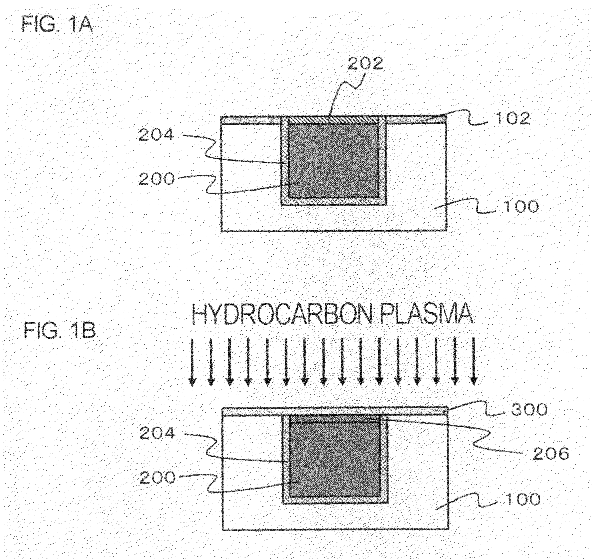
[0026]FIGS. 1A, 1B, 2A and 2B are sectional views showing a method of manufacturing a semiconductor device according to a This method of manufacturing a semiconductor device includes a burying process, a first surface treating process and a film forming process. The burying process is a process of burying a conductive pattern 200 in an insulating film 100 made of SiOH, SiCOH or organic polymer. The first surface treating process is a process of treating surfaces of the insulating film 100 and the conductive pattern 200 with plasma with a treatment gas which includes a hydrocarbon gas. The film forming process is a process of forming a diffusion barrier film 302 formed of an SiCH film, SiCHN film, SiCHO film or SiCHON film over the insulating film 100 and the conductive pattern 200 using a plasma CVD by adding an Si-containing gas to the treatment gas while increasing the addition amount gradually or in a step by step manner. Hereinafter, these processes will be described in detail....

third embodiment

[0046]FIG. 5 is a sectional view showing a configuration of a semiconductor device according to a This semiconductor device has a structure in which an interlayer insulating film 30 and an insulating layer 110 are formed over a substrate 10 on which a transistor 20 is formed and additional insulating layers 120, 130, 140 and 150 are stacked in that order.

[0047]The insulating layer 110 is for example a silicon oxide film and may have the same configuration as the insulating film 100 in the first or second embodiment. A conductive pattern 210 is buried in the insulating layer 110. The conductive pattern 210 has the same configuration as the conductive pattern 200 in the first or second embodiment. The conductive pattern 210 is connected to the transistor 20 through, for example, a contact buried in the interlayer insulating film 30.

[0048]The insulating layers 120, 130 and 140 have the same configuration as the insulating film 100 in the first or second embodiment and are respectively...

second embodiment

[0050]This embodiment can also obtain the same effects as the first or

[0051]Although the various embodiments of the present invention have been shown and described above with reference to the drawings, these embodiments are only examples of the present invention which may employ various other configurations. For example, although the CH film 300 is formed between the insulating film 100 and the conductive pattern 200, and the diffusion barrier film 302 in each of the above embodiments, the CH film 300 does not need to be formed.

[0052]In addition, in the process shown in FIG. 1B, a nitrogen-containing gas (for example NH3, N2 or the like) may be added to the treatment gas. In this case, instead of the CH film 300, a CHN film is formed on the surface of the insulating film 100 and the surface of the conductive pattern 200. In this case, the same effects as above can also be obtained. In addition, since a breakdown voltage of the CHN film is higher than that of the CH film 300, the bre...


PUM

PropertyMeasurementUnit
relative permittivityaaaaaaaaaa
diameteraaaaaaaaaa
distanceaaaaaaaaaa

Abstract

A method includes burying a conductive pattern in an insulating film made of SiOH, SiCOH or organic polymer, treating surfaces of the insulating film and the conductive pattern with plasma which includes a hydrocarbon gas as a treatment gas, and forming a diffusion barrier film, which is formed of an SiCH film, an SiCHN film, an SiCHO film or an SiCHON film, over the insulating film and the conductive pattern with performing a plasma CVD by adding an Si-containing gas to the treatment gas while increasing an addition amount gradually or in a step by step manner.

Description

[0001]This application is based on Japanese patent application NO. 2008-290977, the content of which is incorporated hereinto by reference.BACKGROUND[0002]1. Technical Field[0003]The present invention relates to a semiconductor device including a diffusion barrier film formed over an insulating film and a conductive pattern, and a method of manufacturing the same.[0004]2. Related Art[0005]In recent years, copper has been used as interconnect material for semiconductor devices. Copper interconnect is formed in the form of being buried in an insulating film. When copper is used as interconnect material for semiconductor devices, a diffusion barrier film is required to be formed over the copper interconnect in order to prevent the copper from being diffused to an upper layer of the copper interconnect. When the diffusion barrier film is formed over the copper interconnect, it is necessary to secure adhesion between the copper interconnect and the diffusion barrier film and adhesion bet...

Claims


Application Information

Patent Timeline
Patent Type & Authority Patents(United States)
IPC IPC(8): H01L23/48
CPCH01L21/76822H01L21/76826H01L21/76832H01L21/76883H01L23/53295H01L21/76834H01L2924/30105H01L2924/0002H01L2924/00
Inventor USAMI, TATSUYA
Owner RENESAS ELECTRONICS CORP
Why Eureka
Try Eureka