
Memory card with electrostatic discharge protection and manufacturing method thereof

a memory card and discharge protection technology, applied in the field of memory cards, can solve the problems of esd, permanent damage, and the effect of preventing possible damage to electrical devices

Active Publication Date: 2011-05-24
ORIENT SEMICON ELECTRONICS
View PDF7 Cites 34 Cited by
  • Summary
  • Abstract
  • Description
  • Claims
  • Application Information

AI Technical Summary

Benefits of technology

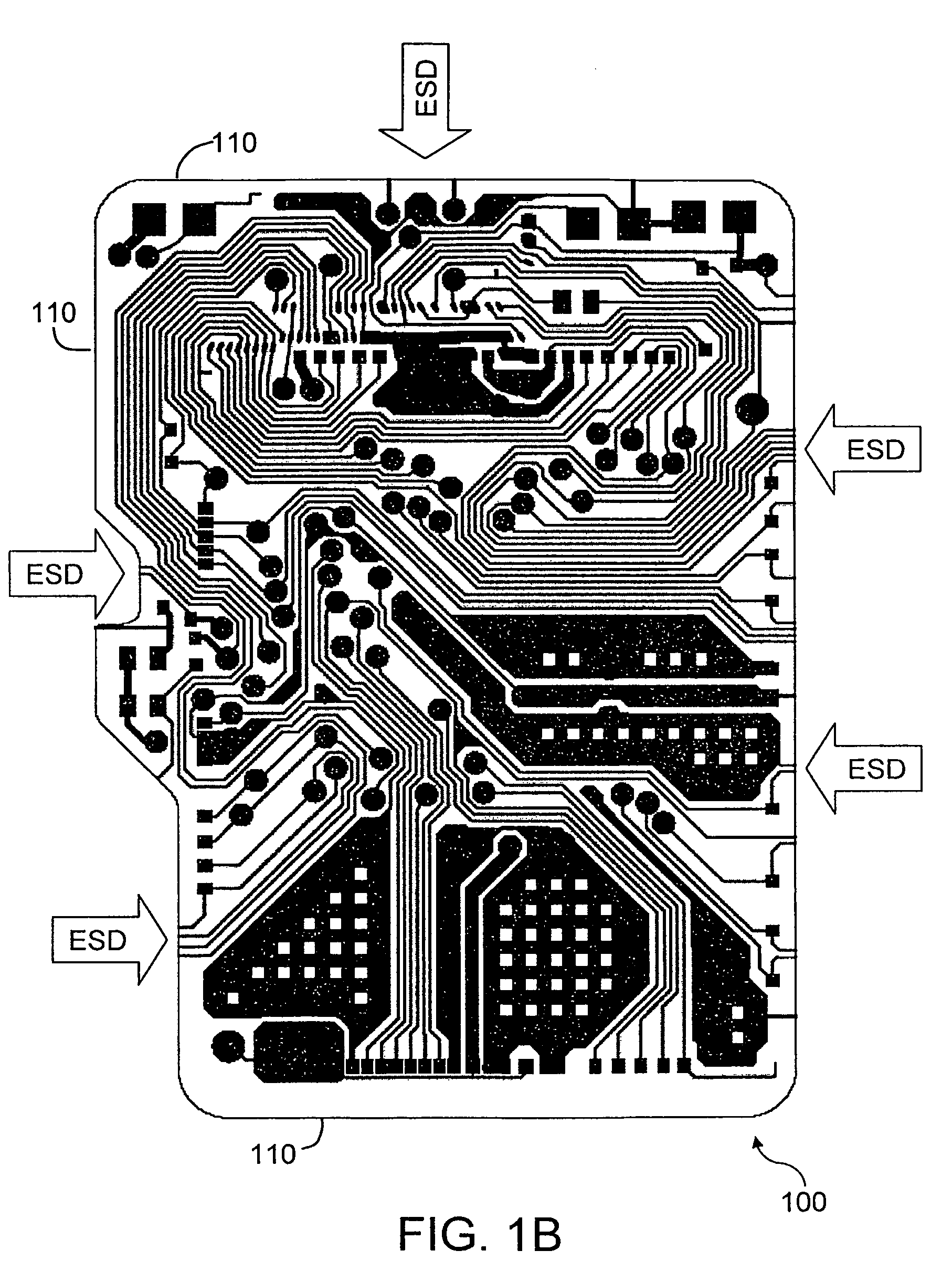
"The present invention provides a memory card with electrostatic discharge (ESD) protection. The memory card includes a circuit board, a set of contacts, at least one chip and an ESD protection path. The ESD protection path is not exposed at the edge of the circuit board, which prevents electrostatic charges from damaging the chips on the circuit board. The ESD protection path includes a metal layer or a ring-shaped area that facilitates the transmission of ESD current out of the circuit board. The invention also provides a method of manufacturing the memory card with ESD protection. The technical effect of the invention is to prevent damage to the electrical devices inside the memory card in an ESD."

Problems solved by technology

An electronic product operating in an actual working environment often encounters the destructive impact of electrostatic discharge (ESD).
If a suitable form of protection is not set up, devices within the electronic product may cause permanent damages.
When an ESD occurs, the ESD current is likely to burn up the internal devices.
Furthermore, the U.S. Pat. No. 5,319,523 does not teach the technique that can prevent electrostatic charges entering the conductive surface traces 56 (signal path) from damaging the components on the printed circuit board.
Similarly, U.S. Pat. No. 6,804,119 does not teach the techniques that ESD protection path extend to the edge of the circuit board and prevent electrostatic charges from entering signal path.
However, as the memory card evolves toward smaller dimension according to the current trend, the casing alone can hardly provide sufficient ESD protective capacity.
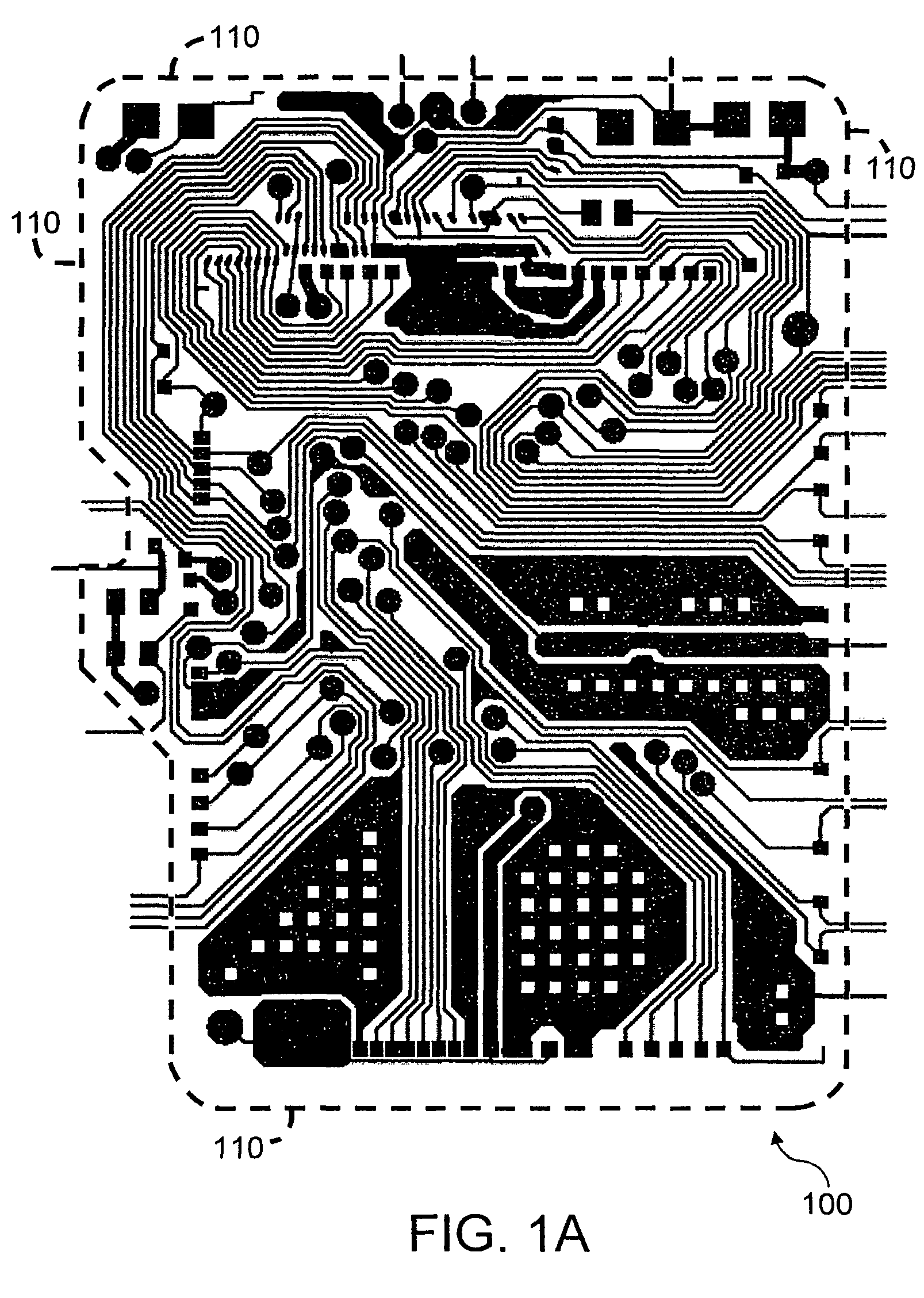
Ultimately, the devices (not shown) on the printed circuit board 100 may be damaged.

Method used


Image

  • Memory card with electrostatic discharge protection and manufacturing method thereof
  • Memory card with electrostatic discharge protection and manufacturing method thereof
  • Memory card with electrostatic discharge protection and manufacturing method thereof

Examples


Embodiment Construction

[0024]Reference will now be made in detail to the present preferred embodiments of the invention, examples of which are illustrated in the accompanying drawings. Wherever possible, the same reference numbers are used in the drawings and the description to refer to the same or like parts.

[0025]To facilitate a comparison with the aforementioned conventional technique, the diagram in FIG. 1A is used as an example of the embodiment in the present invention in the following description. In other words, the processes of fabricating the printed circuit board in the following embodiments include disposing plating lines. However, anyone familiar with the technique may apply the present invention to fabricate other types of printed circuit boards according to the spirit and instruction described in the following embodiments. In other words, whether to dispose the plating lines or not depends on the particular printed circuit board processing technique. Hence, the scope of the present inventio...


PUM

PropertyMeasurementUnit
areaaaaaaaaaaa
electrical insulationaaaaaaaaaa
ESD voltageaaaaaaaaaa

Abstract

A memory card with electrostatic discharge (ESD) protection and a manufacturing method thereof are provided. The memory card includes a circuit board, a set of contacts, at least one chip and an ESD protection path. The signal paths of the board is not exposed at the edge of the circuit board. The ESD protection path for transmitting ESD current is disposed on the circuit board. Furthermore, a part of the ESD protection path extends to the edge of the circuit board.

Description

CROSS-REFERENCE TO RELATED APPLICATION[0001]This is a continuation-in-part application of patent application Ser. No. 11 / 531,000, filed on Sep. 12, 2006, which claims the priority benefit of Taiwan patent application serial no. 95124284, filed on Jul. 4, 2006. The entirety of each of the above-mentioned patent applications is hereby incorporated by reference herein and made a part of this specification.BACKGROUND OF THE INVENTION[0002]1. Field of the Invention[0003]The present invention relates to a memory card, and more particularly, to a memory card with electrostatic discharge protection.[0004]2. Description of Related Art[0005]An electronic product operating in an actual working environment often encounters the destructive impact of electrostatic discharge (ESD). If a suitable form of protection is not set up, devices within the electronic product may cause permanent damages. In general, the ESD voltage is substantially greater than the power source voltage for operating the ele...

Claims


Application Information

Patent Timeline
Patent Type & Authority Patents(United States)
IPC IPC(8): H05K9/00
CPCH05K1/0259H05K2201/09336Y10T29/4913H05K2201/10159H05K2201/09354
Inventor TUNG, YUEH-MINGSUN, KUO-YANGYANG, CHIA-MINGLEE, CHUNG-LUNWEN, JIN-CHUNLIU, YUAN-WEIHUNG, WEI-MAO
Owner ORIENT SEMICON ELECTRONICS
Learn More