Abrupt “delta-like” doping in Si and SiGe films by UHV-CVD

a technology of uhv-cvd and dielectric film, which is applied in the direction of chemistry apparatus and processes, crystal growth process, polycrystalline material growth, etc., can solve the problems of high doping level, undesirable in-situ doping,

Inactive Publication Date: 2011-03-15
GLOBALFOUNDRIES INC
View PDF20 Cites 137 Cited by
  • Summary
  • Abstract
  • Description
  • Claims
  • Application Information

AI Technical Summary

Benefits of technology

The invention further provides a method comprising the steps of selecting a substrate having an upper surface, growing a first epitaxial layer of substantially Ge thereover less than its critical thickness and doped with phosphorus to a level of about 5×10¹⁹ atoms / cc, growing a second epitaxial layer selected from the group consisting of Si and SiGe, the second epitaxial layer having any desired doping profile. The presence of the epitaxial Ge layer accelerates the incorporation rate of the P or As doping into the Ge layer, thereby eliminating the slow transient behavior. The initial, in-situ doping level is determined by the dopant flow in SCCM of the PH3 / He mixture. The final overall doping profile may be controlled as a function of 1 / GR where GR is the growth rate of the first and second layer. The dopant may be supplied or carried by phosphine (PH3) or Tertiary Butyl Phosphine (TBP) gas in the case of P and AsH3 or Tertiary Butyl Arsine (TBA) in the case of As in a UHV-CVD reactor.
To eliminate background “autodoping effect”, the structure with phosphorus doping as shown in FIG. 3 is transferred to a load chamber or load lock, while the growth chamber is purged of the background phosphorus. This growth / interrupt / growth process involves hydrogen flushing of the UHV-CVD reactor during interrupt. Then, a coating of Si or SiGe is grown on the sidewalls and / or heated surfaces of the UHV-CVD reactor at high temperature to isolate, eliminate or cover the residual phosphorus atoms prior to reintroducing the structure for further deposition. Alternatively, a second growth chanber i.e. UHV-CVD reactor coupled to the load chamber may be used where further undoped layers may be deposited with very low levels of phosphorus.

Problems solved by technology

Another well known problem associated with in-situ phosphorus or boron doping in silicon CVD is its “memory effect” as shown by curve portion 15-16 in FIG. 1 for the case of phosphorus herein which tends to create an undesirable high level of dopant in the background due to its “autodoping behavior”.
Hence, in-situ doping typically generates a very undesirable “smearing out” of the dopant profile in silicon films formed by CVD.

Method used


Image

  • Abrupt “delta-like” doping in Si and SiGe films by UHV-CVD
  • Abrupt “delta-like” doping in Si and SiGe films by UHV-CVD
  • Abrupt “delta-like” doping in Si and SiGe films by UHV-CVD

Examples


Embodiment Construction

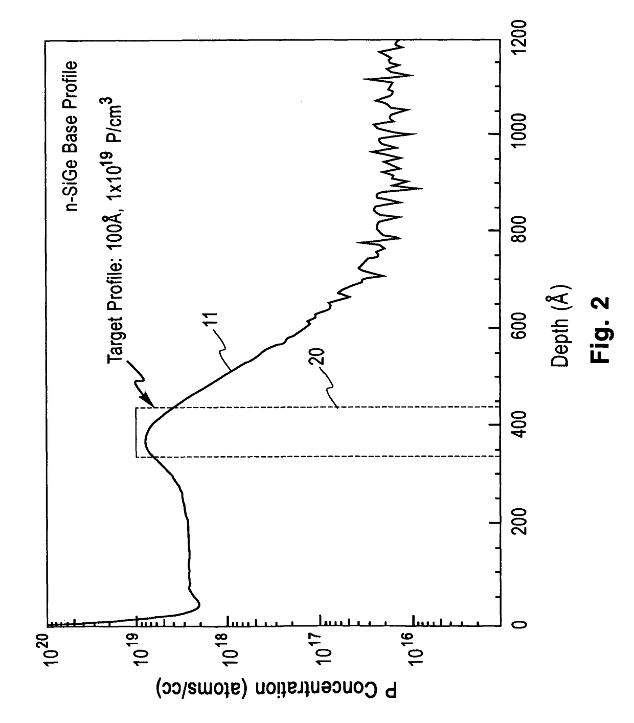
Referring to the drawing and in particular to FIG. 3, a cross section view of structure 30 having an abrupt phosphorus or arsenic profile or abrupt layer doping (ALD) is shown. A substrate 32 having an upper surface 33 may be for example single crystal Si or SiGe. A first layer 36 of 100% or substantially Ge is epitaxially formed on upper surface 33 having a thickness less than the critical thickness and may be, for example, 0.5 to 2 nm and is doped with P or As.

The effect of the thickness of first layer 36 is not to increase the doping concentration of P or As, but the effect is to increase the sheet dose, which is the doping concentration multiplied by the doped layer thickness. The doping concentration is controlled by the flow rate of the dopant source gas and by the growth rate of first layer 36, which in turn, is controlled by the flow rate of the Ge source gas which may be, for example, GeH4.

The critical thickness of a layer is the thickness after which the layer relaxes to r...


PUM

PropertyMeasurementUnit
concentrationaaaaaaaaaa
widthaaaaaaaaaa
widthaaaaaaaaaa

Abstract

A structure and method of forming an abrupt doping profile is described incorporating a substrate, a first epitaxial layer of Ge less than the critical thickness having a P or As concentration greater than 5×10¹⁹ atoms / cc, and a second epitaxial layer having a change in concentration in its first 40 from the first layer of greater than 1×10¹⁹ P atoms / cc. Alternatively, a layer of SiGe having a Ge content greater than 0.5 may be selectively amorphized and recrystalized with respect to other layers in a layered structure. The invention overcomes the problem of forming abrupt phosphorus profiles in Si and SiGe layers or films in semiconductor structures such as CMOS, MODFET's, and HBT's.

Description

FIELD OF THE INVENTIONThis invention relates to semiconductor films with steep doping profiles and more particularly to forming abrupt “delta-like” doping in thin layers from 5-20 nm thick suitable for Si or SiGe CMOS, modulation-doped field-effect transistors (MODFET's) devices, and heterojunction bipolar transistors (HBT's) using in-situ doping in a ultra high vacuum-chemical vapor deposition (UHV-CVD) reactor.BACKGROUND OF THE INVENTIONIn-situ phosphorus doping in epitaxial Si and SiGe films or layers using PH3 has been known to demonstrate a very slow incorporation rate of P due to the “poisoning effect” of phosphine on the Si(100) surface. An example of such a doping behavior is shown in FIG. 1 by curve 11. Curve portion 13-14 of curve 11 shows the slow “transient” trailing edge observed in the SIMS profile and corresponds to the slow incorporation rate of P into the silicon film. In FIG. 1 the ordinate represents P concentration in atoms / cc and the abscissa represents depth in...

Claims


Application Information

Patent Timeline
Patent Type & Authority Patents(United States)
IPC IPC(8): H01L31/0376C30B29/08H01L21/205H01L21/265H01L21/335H01L21/336H01L21/338H01L29/10H01L29/36H01L29/778H01L29/812
CPCH01L21/02381H01L21/0245H01L21/02532H01L21/02576H01L21/0262H01L21/26506H01L29/1054H01L29/36H01L29/41783H01L29/66431H01L29/66477H01L29/66575H01L29/6659H01L29/66628H01L29/7833H01L29/665H01L21/18
Inventor CARDONE, FRANKCHU, JACK OONISMAIL, KHALID EZZELDIN
Owner GLOBALFOUNDRIES INC
Why Eureka
Try Eureka