Optimal local supply voltage determination circuit

a local supply voltage and determination circuit technology, applied in the field of semiconductor circuits, can solve the problem that the power-saving potential of the local supply voltage within a given local supply island may be too optimistic, and achieve the effect of reducing the probability of failure to meet the requirements of the local supply voltage tes

Inactive Publication Date: 2011-03-01
INT BUSINESS MASCH CORP
View PDF10 Cites 11 Cited by
  • Summary
  • Abstract
  • Description
  • Claims
  • Application Information

AI Technical Summary

Problems solved by technology

Further, reduction of heat generation from the local voltage islands may enable faster operation of the rest of the semiconductor chip since the operation of the overall semiconductor chip is limited by the total amount of heat generation.
Further, the design point for the local supply voltage within a given local voltage island may turn out to be too optimistic, in which case the full power-savings potential of the local supply voltage within a given local voltage island may turn out to be too pessimistic, in which case the circuit within the local voltage island is not fully functional at a nominal operation voltage, i.e., the semiconductor chip may operate only above the nominal operation voltage at which the local voltage island is provided with a higher voltage than the voltage at the design point.

Method used


Image

  • Optimal local supply voltage determination circuit
  • Optimal local supply voltage determination circuit
  • Optimal local supply voltage determination circuit

Examples


Embodiment Construction

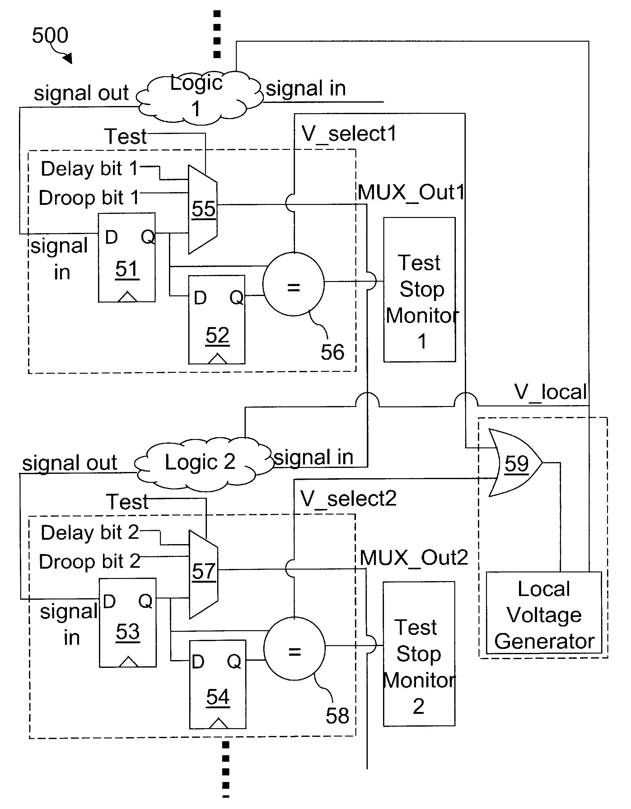
[0062]As stated above, the present invention relates to a semiconductor circuit for determining an optimal local supply voltage for a voltage island in a semiconductor chip, and methods of operating the same, which are now described in detail with accompanying figures. It is noted that like and corresponding elements are referred to by like names or reference numerals in the figures.

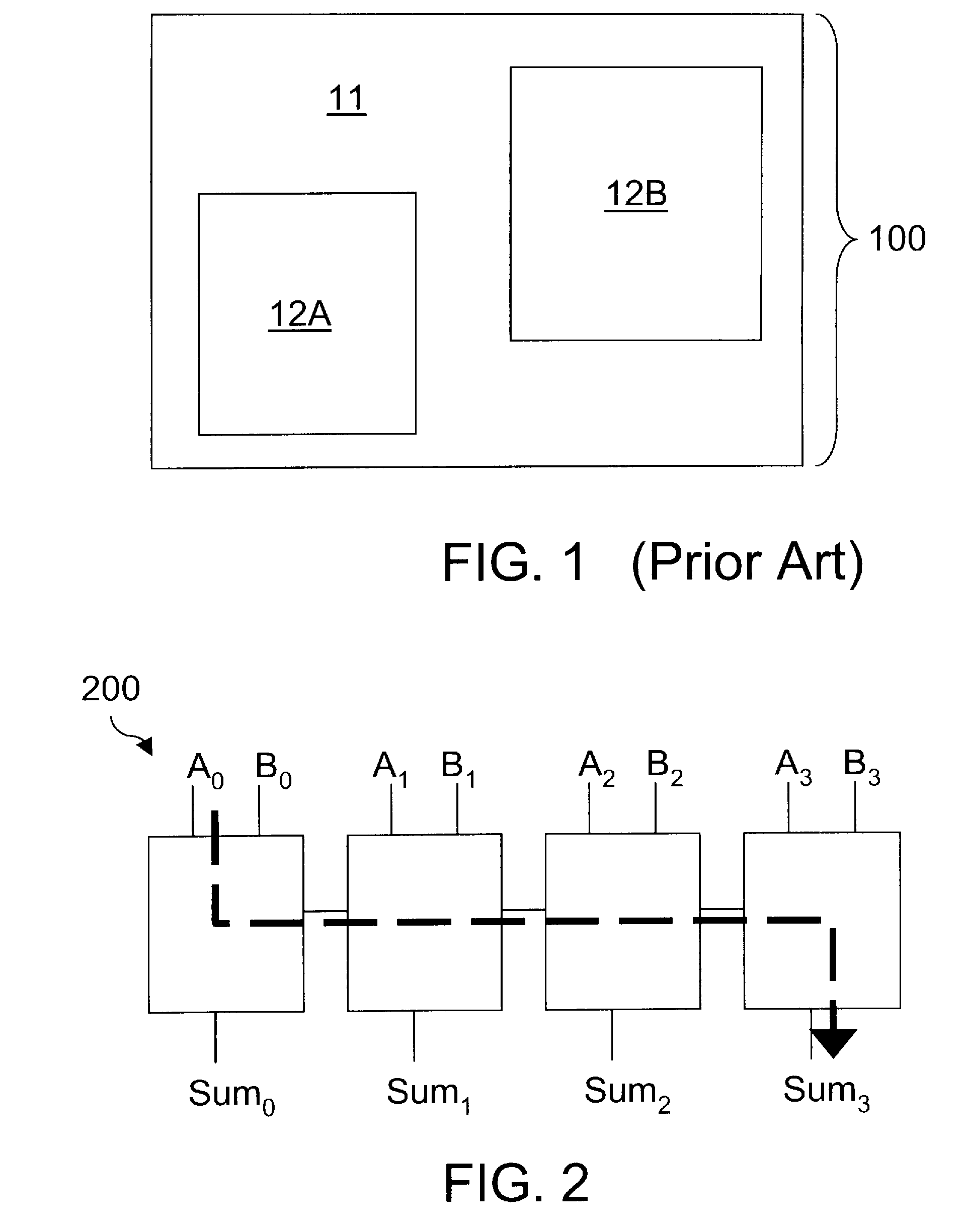
[0063]Referring to FIG. 2, an exemplary 4-bit adder 200 comprises four logic units, each of which is provided with two input nodes and an output node. The concepts of a critical delay path, a critical delay path test vector, and a critical voltage droop test vector, which are developed in the present invention and applicable to general semiconductor logic circuits, are illustrated with the exemplary 4-bit adder 200.

[0064]A carryover node between adjacent logic units provides a signal path for relaying a carryover bit from one logic unit to another. The exemplary 4-bit adder 200 is capable of adding a fir...


PUM


Abstract

A test circuit that compares test results between two tests with different local supply voltages is provided. The output of each stage of the logic circuits is stored in a first register of each test circuit. Each test is performed with a critical test vector and a local supply voltage that decreases from test to test. The outputs of successive tests are compared in each test circuit. The tests are performed iteratively with successive reduction in the value of the local supply voltage until at least one stage of the logic circuits produces non-matching results between the first and second register. The voltage immediately before producing such non-matching results is the minimum operational voltage for the local voltage island.

Description

FIELD OF THE INVENTION[0001]The present invention relates to a semiconductor circuit for determining an optimal local supply voltage for a voltage island in a semiconductor chip, and methods of operating the same.BACKGROUND OF THE INVENTION[0002]Many high performance semiconductor chips and low power semiconductor chips employ local voltage islands that employ a reduced power supply voltage compared to the rest of a semiconductor chip. FIG. 1 shows a prior art semiconductor chip 100 that employs a regular supply voltage region 11, a first local voltage island 12A, and a second local voltage island 12B. Within each of the local voltage islands (12A, 12B), a local power supply voltage, which is lower than the power supply voltage employed in the regular supply voltage region 11, is provided to the semiconductor circuitry therein. As an illustrative example, circuits in the regular supply voltage region 11 may employ 1.5 V, circuits in the first local voltage island may employ 1.2 V, a...

Claims


Application Information

Patent Timeline
Patent Type & Authority Patents(United States)
IPC IPC(8): H03K19/00
CPCG01R31/3004
Inventor BERNSTEIN, KERRYWOLPERT, DAVID S.
Owner INT BUSINESS MASCH CORP
Why Eureka
Try Eureka