
Dye for photoelectronic device, photoanode comprising the dye and photoelectronic device employing the photoanode

a technology of photoelectronic devices and dyes, which is applied in the direction of discharge tubes/lamp details, natural mineral layered products, synthetic resin layered products, etc., can solve the problems of unmet needs in the art, the improvement of cell efficiency, and the limitation of the practical application of cells, so as to improve light absorption efficiency and good sensitivity to sunlight

Inactive Publication Date: 2011-01-04
SAMSUNG SDI CO LTD
View PDF1 Cites 0 Cited by
  • Summary
  • Abstract
  • Description
  • Claims
  • Application Information

AI Technical Summary

Benefits of technology

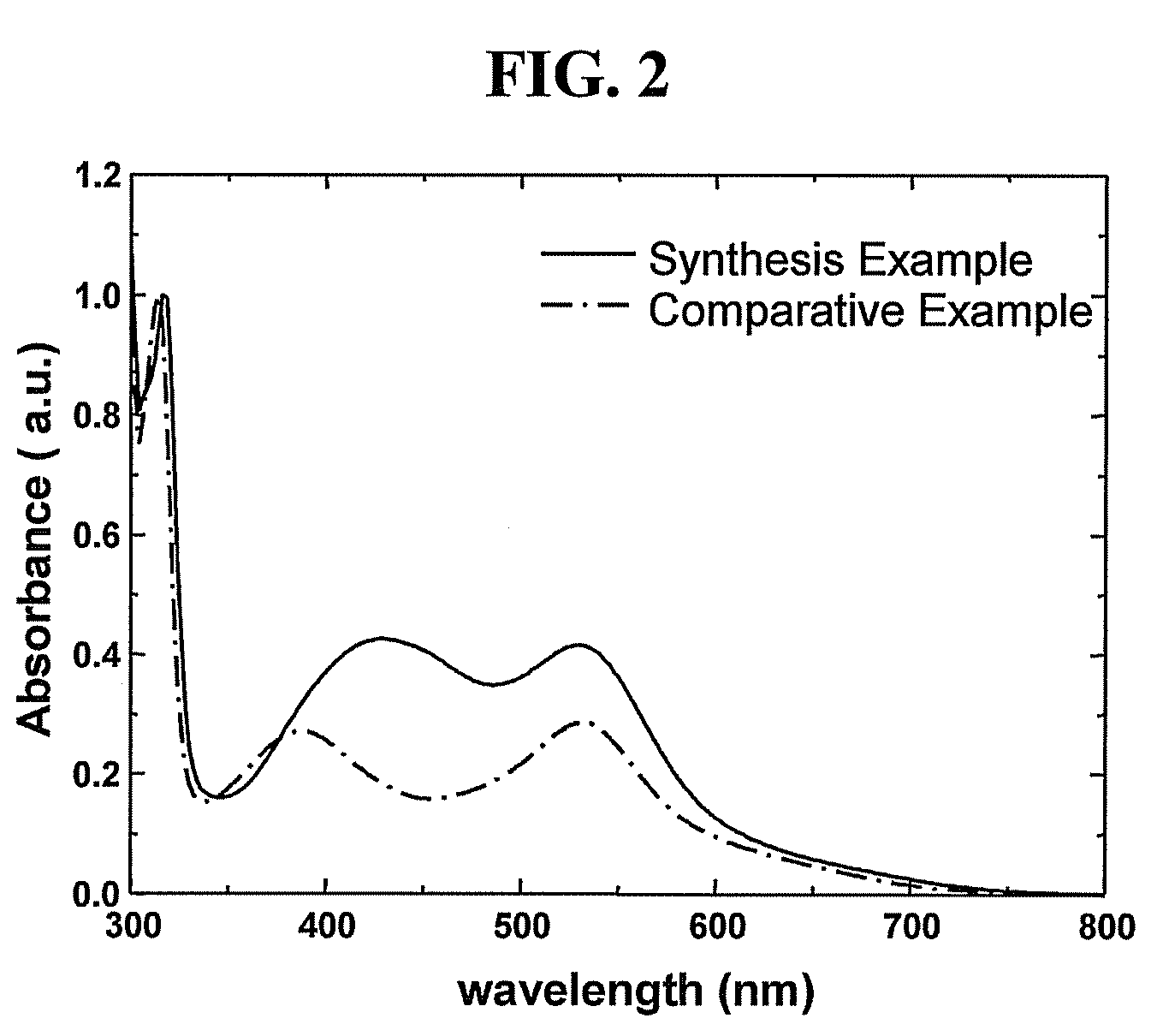
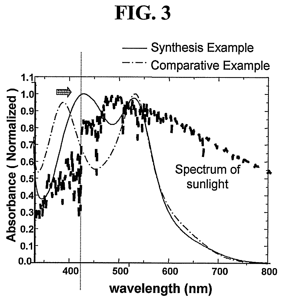
[0012]In one embodiment, the present invention provides a novel dye for use in a photoelectronic device that has good sensitivity to sunlight, and absorbs sunlight at a broad range of wavelengths, resulting in improved light absorption efficiency.
[0013]In another embodiment, the present invention provides a photoanode with high power conversion efficiency, which comprises the dye.
[0014]In yet another embodiment, the present invention provides a photoelectronic device, with high power conversion efficiency, comprising the photoanode.

Problems solved by technology

However, since silicon solar cells are expensive to manufacture, there are some limitations in regards to the practical application of the cells and the improvement in the efficiency of the cells.
However, there is still an unmet need in the art to develop a dye that exhibits improved absorption properties.

Method used


Image

  • Dye for photoelectronic device, photoanode comprising the dye and photoelectronic device employing the photoanode
  • Dye for photoelectronic device, photoanode comprising the dye and photoelectronic device employing the photoanode
  • Dye for photoelectronic device, photoanode comprising the dye and photoelectronic device employing the photoanode

Examples


synthesis example 1

Synthesis of the Dye

[0050]

A solution of 4,7-Diphenyl-1,10-phenanthroline (266 mg, 0.8 mMol) and dichloro(p-cymene)ruthenium(II) dimmer (240 mg, 0.2 mMol) in 50 ml (milliliters) of dimethylformamide (‘DMF’) was refluxed under a nitrogen atmosphere at 100° C. for 4 hours. After 4,4′-dicarboxy-2,2′-bipyridine (216 mg, 0.8 mmol) was added to the solution, the mixture was refluxed at 160° C. for 4 hours. Ammonium thiocyanate (NH4NCS) (608 mg, 8 mmol) was added to the hot mixture and refluxed at 140° C. for 4 hours. Subsequently, the resulting mixture was allowed to cool to room temperature and the solvent was removed by distillation under reduced pressure to obtain a purple solid precipitate. The precipitate was added to 300 ml of water and dissolved by sonication for 5 minutes. The pH of the solution was adjusted to pH 4 by the addition of a 0.2 M nitric acid (HNO3) solution. The acidic solution was subsequently allowed to stand in a freezer for one day to obtain a precipitate. The prec...

example 1

Production of a Photoanode and Fabrication of a Photoelectronic Device

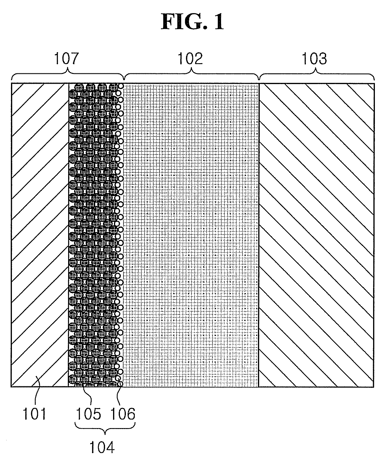
[0053]After fluorine-doped tin oxide (FTO) was applied to a glass substrate using a sputter coater, a paste of TiO2 particles (particle diameter: 13 nm) was coated thereon by screen printing, and then baked at 450° C. for 30 minutes to form a porous TiO2 film having a thickness of about 15 μm (micrometers). Subsequently, the glass substrate, on which the TiO2 film was formed, was dipped in a 0.3 mM solution of the dye (Synthesis Example 1), prepared in a mixture of butanol and acetonitrile (1:1 (v / v)), for 24 hours and then dried to allow the dye to adsorb on the surface of the TiO2 layer, thereby completing production of a photoanode.

[0054]Next, platinum was deposited on a glass substrate coated with indium tin oxide (ITO) using a sputter coater to form a platinum film, and thereafter, a fine hole for injection of an electrolyte was formed thereon using a drill (diameter: 0.75 mm) to produce a cathode.

[0055]The p...


PUM

PropertyMeasurementUnit
pHaaaaaaaaaa
heightaaaaaaaaaa
thicknessaaaaaaaaaa

Abstract

Disclosed is a novel dye for use in a photoelectronic device, wherein the photoelectronic device is comprised of a photoanode comprising the dye. According to the novel dye, the dye is derived through the introduction of a group which narrows the dihedral angle of the dye ligand as well as through the introduction of conjugated groups. Since the dye has improved light sensitivity and absorption properties, it can be used to fabricate a photoelectronic device with high power conversion efficiency.

Description

CROSS-REFERENCE TO RELATED PATENT APPLICATION[0001]This non-provisional application claims priority to Korean Patent Application No. 10-2006-0079311, filed on Aug. 22, 2006, and all the benefits accruing therefrom under 35 U.S.C. §119, the content of which in its entirety is hereby incorporated by reference.BACKGROUND OF THE INVENTION[0002]1. Field of the Invention[0003]The present invention relates to a novel dye for use in a photoelectronic device, wherein the photoelectronic device is comprised of a photoanode comprising the dye. More specifically, the present invention relates to a novel dye for use in a photoelectronic device in which the dye is derived through the introduction of a group that narrows the dihedral angle of the dye ligand as well as the introduction of conjugated groups. The resulting novel dye has increased light sensitivity and absorption efficiency.[0004]2. Description of the Related Art[0005]In recent years, numerous studies have focused on various alternati...

Claims


Application Information

Patent Timeline
Patent Type & Authority Patents(United States)
IPC IPC(8): C07F15/00H01L31/0256
CPCC07F15/0053C09B57/10H01G9/2031H01G9/2059H01G9/2004Y02E10/542Y10T428/31507Y10T428/31938C09B45/04C09B45/14C09B45/22C09B45/32
Inventor SOHN, BYUNG HEEPARK, SANG CHEOLJUNG, WON CHEOLNAM, JUNG GYUPARK, YOUNG JUNLEE, EUN SUNG
Owner SAMSUNG SDI CO LTD
Learn More