Current source circuit

a current source circuit and current source technology, applied in the direction of electric variable regulation, process and machine control, instruments, etc., can solve the problems of affecting the normal operation of the entire circuit, the circuit cannot be implemented on the glass substrate, and the operation of the circuit is affected, so as to achieve the effect of more precise bias current of the current source circui

Inactive Publication Date: 2010-10-05
CHUNGHWA PICTURE TUBES LTD
View PDF6 Cites 0 Cited by
  • Summary
  • Abstract
  • Description
  • Claims
  • Application Information

AI Technical Summary

Benefits of technology

[0009]The present invention is directed to a current source circuit adapted for minimizing the effect of the threshold voltage on the bias current to ensure the bias current of the current source circuit is more precise.
[0012]Through the voltage divider module and the current mirror module, the present invention ensures the first transistor operates in the sub-threshold region to effectively minimize the threshold voltage variation and the bias current outputted by the second transistor being more precise. Further, when the circuit is in operation, no defect such as the non-uniform performance is resulted to affect the overall performance of the circuit.

Problems solved by technology

During the LTPS fabrication process, if the bias voltage is not precise enough, the circuit cannot be implemented on the glass substrate.
Defects such as non-uniform performance may result in LTPS fabrication process, which the threshold voltage may be varied and the bias voltage become made imprecise, thus the operation of the circuit is affected.
This variation will result in mismatch between the gate voltage VG and the drain current ID, affecting the normal operation of the entire circuit.
Therefore, variation in the threshold voltage affects the operation of the entire circuit.

Method used


Image

  • Current source circuit
  • Current source circuit
  • Current source circuit

Examples


Embodiment Construction

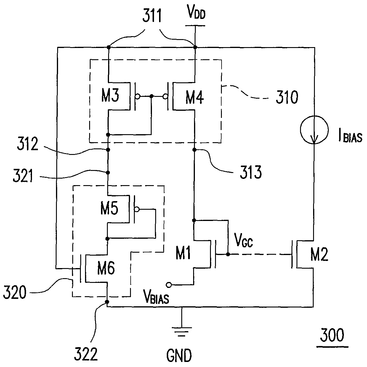
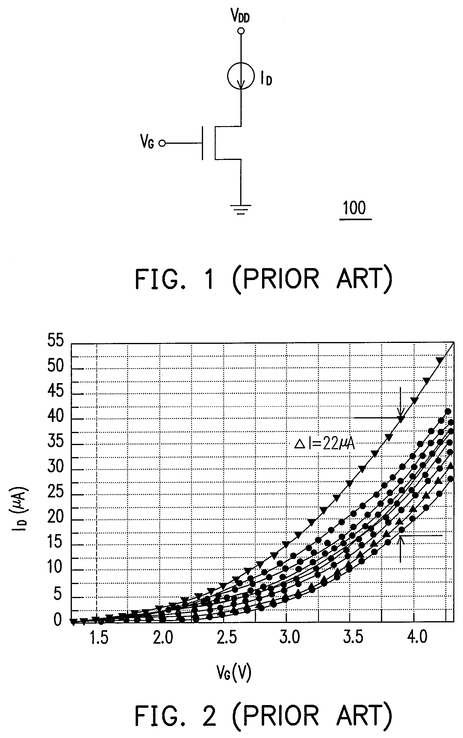
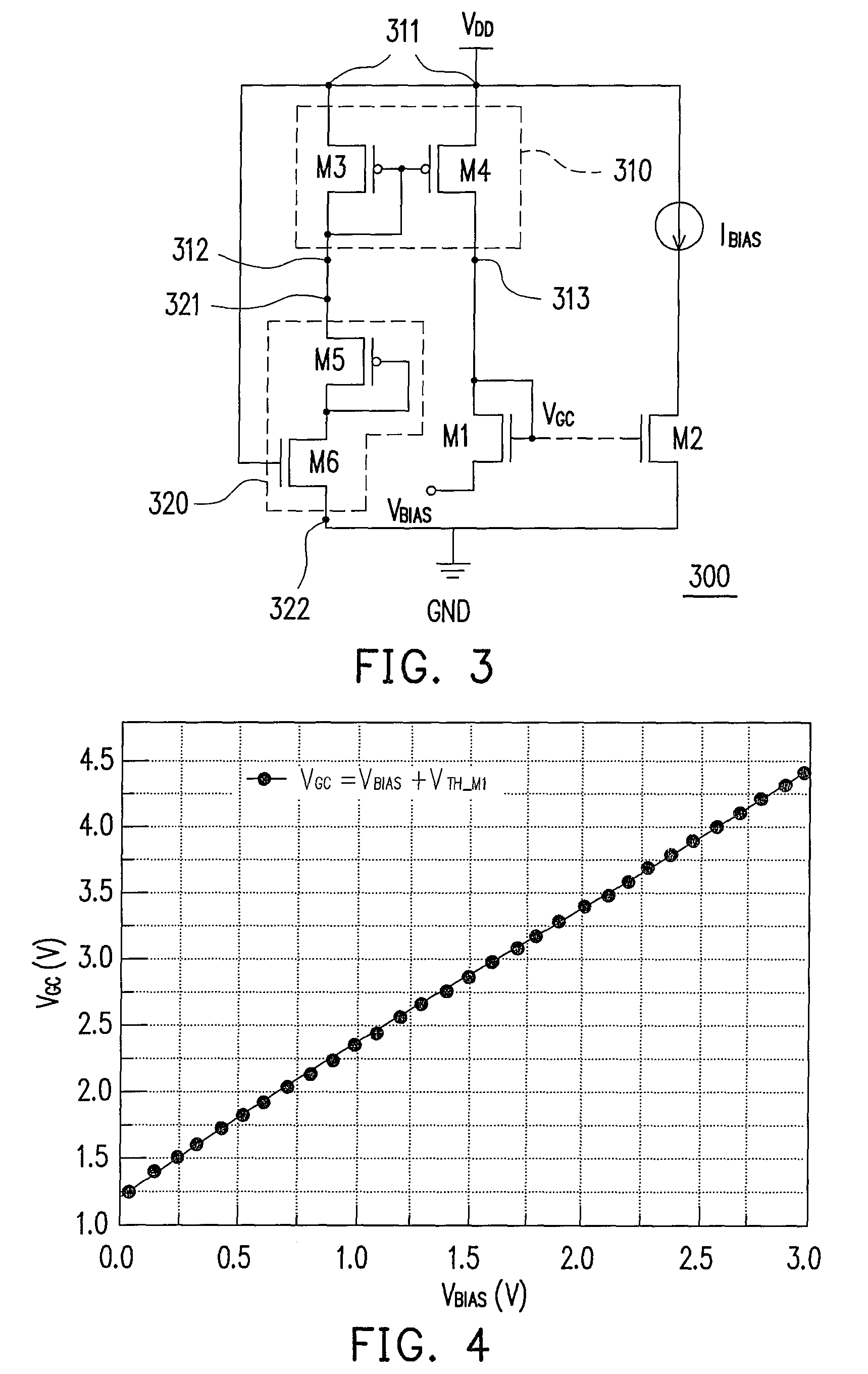
[0022]Generally, a transistor mounted on a glass substrate usually operates in the saturation region. In LTPS fabrication process, the transconductance gm and the output resistance ro of the transistor determines the small signal gain and the frequency response of the analog circuit. The parameters of the transconductance gm and the output resistance ro of the transistor are described as the equations listed below:

[0023]gm=μ⁢⁢Cox⁢WL⁢(VGS-VTH)=2⁢ID(VGS-VTH)(1)

[0024]ro=VAID(2)

[0025]When the transistor is operated in the saturation region, the drain current ID may be described as the equation listed below:

[0026]ID=μ⁢⁢Cox⁢WL⁢(VGS-VTH)2(3)

[0027]Herein, Equation (3) has not taken the channel length modulation effect and the body effect into consideration. In Equation (3), the threshold voltage of the transistor is an important parameter. If the threshold voltage varies, the drain current ID varies as well, lowering the performance of the analog circuit on the glass substrate. Hence, the p...


PUM


Abstract

A current source circuit is provided. The circuit includes a first transistor and at least one second transistor. A first source / drain terminal of the first transistor is coupled to a bias voltage. A second source / drain terminal of the first transistor is used to receive a current signal, and the second source / drain terminal of the first transistor is coupled to a gate terminal of the first transistor. A first source / drain terminal of the second transistor is grounded. A second source / drain terminal of the second transistor is coupled to a voltage source and outputs a bias current. A gate terminal of the second transistor is coupled to the gate terminal of the first transistor.

Description

CROSS-REFERENCE TO RELATED APPLICATION[0001]This application claims the priority benefit of Taiwan application serial no. 96119579, filed on May 31, 2007. The entirety of the above-mentioned patent application is hereby incorporated by reference herein and made a part of this specification.BACKGROUND OF THE INVENTION[0002]1. Field of the Invention[0003]The present invention relates to a current source circuit, and more particularly, to a current source circuit having a compensation threshold voltage.[0004]2. Description of Related Art[0005]Low-temperature poly-silicon (LTPS) technology is a new fabrication processing technology for thin film transistor liquid crystal displays (TFT-LCD). In comparison with conventional amorphous silicon (a-Si) LCD, a LTPS LCD has the advantages of fast response speed, high brightness and high resolution.[0006]Hence, the use of LTPS transistor for application in integrated circuits such as active matrix liquid crystal display (AMLCD) and active matrix...

Claims


Application Information

Patent Timeline
Patent Type & Authority Patents(United States)
IPC IPC(8): G05F1/10G05F3/02
CPCG05F3/242
Inventor KER, MING-DOUCHEN, JUNG-SHENGHSU, CHUN-YUAN
Owner CHUNGHWA PICTURE TUBES LTD
Why Eureka
Try Eureka