
Method and electrode for defining and replicating structures in conducting materials

a technology of conducting materials and electrodes, applied in the field of new etching or plating methods, can solve the problems of high equipment costs, lack of selectivity, and problems with redeposition on samples, and achieve the effect of simplifying the production of applications

Inactive Publication Date: 2010-09-07
REPLISAURUS GROUP
View PDF27 Cites 21 Cited by
  • Summary
  • Abstract
  • Description
  • Claims
  • Application Information

AI Technical Summary

Benefits of technology

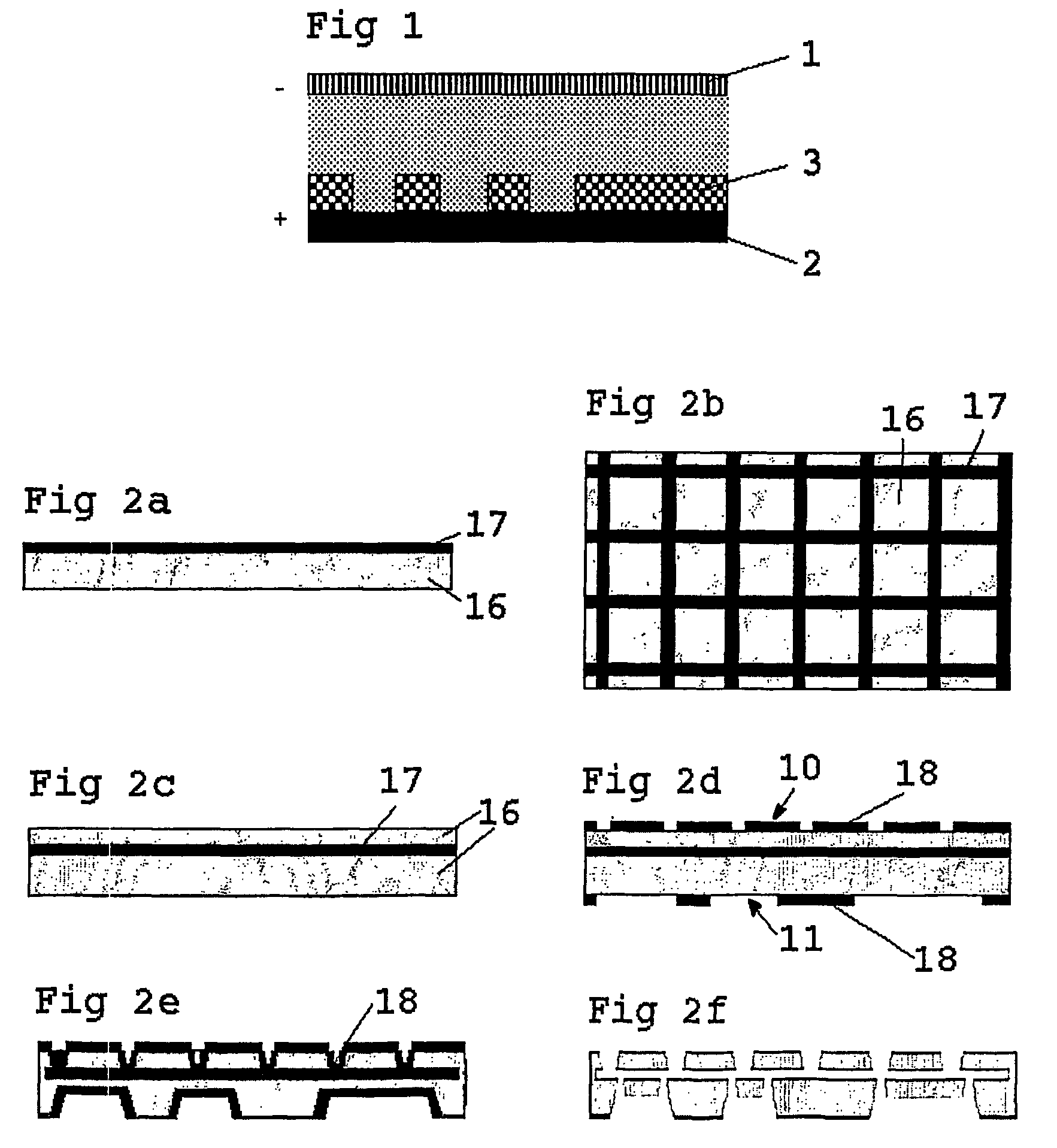
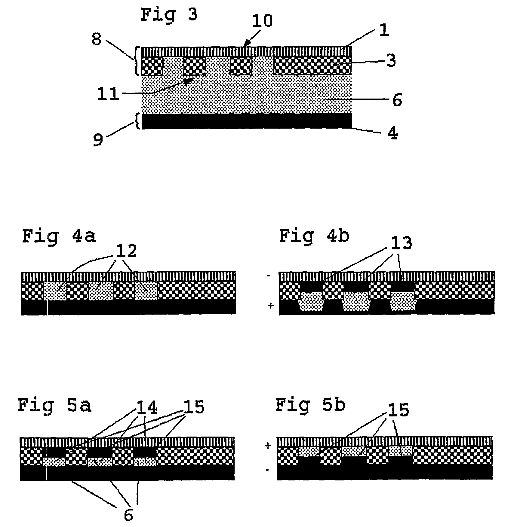
"The present invention provides a method for producing micro and nano structures using a special contact electrochemical etching / plating method called the electrochemical pattern replication (ECPR) method. This method allows for the accurate control of electrochemical etching or plating processes without limitations in maximum aspect ratio of deposited structures, variations in material composition of deposits, and reliability problems in large scale production. The method also eliminates the need for a subsequent planarization process and solves the problem of differences in deposition speed depending on the pattern being plated. The master electrode used in the ECPR method can be designed to operate both as a counter electrode and pattern master, allowing for the production of multiple replicas in conducting materials. The technical effects of the invention include simplifying production processes, improving process control, and reducing costs."

Problems solved by technology

Some of the disadvantages of dry etching are high equipment costs, lack of selectivity, problems with redeposition on the sample, environmentally hazardous chemicals, surface damages on the etched sample and safety and disposal problems.
One of the disadvantages is that it does not involve any directional driving force and therefore the etching rate is the same in all directions, which results in an isotropic etchprofile.
Some other disadvantages are that wet etching baths generally contain aggressive and toxic chemicals, which results in safety and disposal problems.
In many wet etching processes waste treatment and disposal costs often surpass actual etching costs, and the same drawback applies for dry etching.
One problem the designers of electrochemical etching cells are facing is that, to reduce the resistive losses from charge transfer in the electrolyte, one wants a small electrode distance.
The result is that some parts of the sample are over-etched while some parts are not etched to the desired depth.
No mechanical support is possible to keep the electrode in position over the whole surface, since no contact between sample and counter electrode is allowed.
Another problem in electrochemical etching is non-uniform current density distribution arising from accumulated currents from non-etched areas, due to the fact that all parts of the counter electrode are in contact with the electrolyte, and not only the desired areas, above the etched parts.
However, common industrial problems are associated with the known electroplating process, namely non uniform current density distribution resulting in a deposition rate depending on the pattern surrounding each structure that is plated.
Furthermore, such differences in current density also result in different material composition when plating alloys, as well as differences in height of electroplated structures on a substrate.
The complicated nature of the pattern defining lithography process and the large number of lithography steps needed to fabricate a micro-device makes it to a major time and cost carrier in the total manufacturing chain.
The electrodes according to EP 1060299 have to be transparent to electromagnetic radiation and they do not compensate for unevenness in the micro / nano areas.
However, the disclosed method struggles with the same problems and drawbacks as associated with conventional electroplating, namely non-uniform plating rates as a result of non-uniform current density distribution due to the anode having areas with a surface size differing from the surface size of corresponding cathode areas on the patterned substrate.
When plating alloys, the method described in WO9845504 suffers from the same problems as conventional plating processes, namely differences in material composition because of non uniform current density distribution.
Furthermore, the mentioned embodiment disclosed in WO 9845504 requires an electroplating article fabricated with a porous material that is permeable for ions in the electrolyte, which gives rise to limitations in how small dimensions that can be defined, depending on the pore size of the material.
However, the problem of non uniform current density distribution also applies to this method, as the patterned mask still is placed as a separate layer onto the anode layer, i.e. the current density distribution is only at the beginning of a plating process uniform, whereas the contact surface of the electrolyte with the anode material increases differently in each local plating cell, depending on its size, as anode material is consumed.
Moreover, the maximum aspect ratio, i.e. height / width ratio, of structures that can be plated is limited by the fact that the erosion of the anode material in the electroplating article undercuts the insulating pattern mask.
Undercutting the mask layer during use is also associated with reliability problems, since the patterned mask layer will be completely undercut and disintegrated from the electroplating article if the electroplating process is not terminated in time.
The problems described are inherently associated with the method because the soluble anodic material is transferred directly from the electroplating article itself, even in the case where the electroplating article consists of different layers of soluble and insoluble material.

Method used


Image

  • Method and electrode for defining and replicating structures in conducting materials
  • Method and electrode for defining and replicating structures in conducting materials
  • Method and electrode for defining and replicating structures in conducting materials

Examples


first embodiment

[0103]The first embodiment, which is shown in FIG. 8, is based on a membrane solution where a pressurised membrane 24 is expanded against the master electrode 8 or the substrate 9. The medium 19 inside the pressure volume can be both gas and liquid. Gas bubbles are eliminated by a combination of ultrasound and vacuum, or just using ultrasound. In this embodiment electrical contact to the master electrode 8 is provided from the outer side 10, i.e. from the membrane 24 and contact to the substrate 9 from the front side. Plane parallelism is ensured by the nature of the expanding membrane, applying an even pressure in a conformable way. Both flexible and rigid master electrodes and substrates can be used in this embodiment.

second embodiment

[0104]The second embodiment is based on a cylinder, which is shown in FIG. 9, containing a moveable piston, not shown in the figure. The entire system is confined. Pressure is applied to compress the two electrodes 8, 9 pneumatically using a combination of vacuum and overpressure or hydraulically using a hydraulic piston or mechanically using a screw. Gas bubbles are eliminated by a combination of ultrasound and vacuum. In this embodiment electrical contact 26 to the master electrode is provided from the outer side 10 and contact to the substrate 25 from the front side using conducting movable rods. Plane parallelism is ensured by two flexible elastomer layers between the sample and the piston, one being more compressible than the other is. These elastomer layers can also be placed behind the master electrode 8, i.e. between master electrode and cylinder wall. Both flexible and rigid master electrodes and substrates can be used in this embodiment.


PUM

PropertyMeasurementUnit
frequencyaaaaaaaaaa
frequencyaaaaaaaaaa
widthaaaaaaaaaa

Abstract

The present invention concerns an electrochemical pattern replication method, ECPR, and a construction of a conductive electrode for production of applications involving micro and nano structures. An etching or plating pattern, which is defined by a conductive electrode, a master electrode, is replicated on an electrically conductive material, a substrate. The master electrode is put in close contact with the substrate and the etching / plating pattern is directly transferred onto the substrate by using a contact etching / plating process. The contact etching / plating process is performed in local etching / plating cells, that are formed in closed or open cavities between the master electrode and the substrate.

Description

[0001]This application is a continuation of PCT Application PCT / SE02 / 01179 filed on Jun. 17, 2002, which claims priority to Swedish Patent Application 0102144-3 filed on Jun. 15, 2001.TECHNICAL FIELD[0002]The present invention relates to a new etching or plating method for simplifying production of applications involving micro and nano structures by using a special electrode, according to the appended claims.[0003]The present invention is closely related to electrochemical etching, plating, photolithography and pattern replication and is within the micro- and nanotechnic area.[0004]The method is particularly useful for fabrication of PWB (printed wiring boards), PCB (printed circuit boards), MEMS (micro electro mechanical systems), sensors, flat panel display, magnetic and optical storage devices. Integrated circuits, different types of structures in conductive polymers, structures in semiconductors, structures in metals, and others are possible to produce using this method. Even 3D...

Claims


Application Information

Patent Timeline
Patent Type & Authority Patents(United States)
IPC IPC(8): C25D5/02C25B9/19C25D7/00C25D7/12C25D5/22C25F3/14H05K3/07H05K3/20
CPCC25D5/02C25D7/12C25F3/14H05K3/205H05K3/07H05K3/00H05K2203/0117B82Y10/00C25F3/02
Inventor MOLLER, PATRIKFREDENBERG, MIKAELWIWEN-NILSSON, PETER
Owner REPLISAURUS GROUP
Learn More