
Integrated circuit for driving semiconductor device and power converter

a technology of integrated circuits and semiconductor devices, which is applied in the direction of substation/switching arrangement details, power conversion systems, semiconductor/solid-state device details, etc., can solve the problems of reducing the chip size, affecting and affecting so as to improve the reliability of noise immunity, the chip area is increased, and the development period and cost of semiconductor chips are reduced

Inactive Publication Date: 2010-07-27
HITACHI LTD
View PDF27 Cites 12 Cited by
  • Summary
  • Abstract
  • Description
  • Claims
  • Application Information

AI Technical Summary

Benefits of technology

The patent text discusses the challenges of producing driver circuits in the IC form, which can meet the demands of higher output, higher voltage, and smaller loss. The technical problem addressed by the patent is to address these challenges and limitations of current production methods. The patent proposes a solution to improve the heat releasing ability, reduce the inductance residing in the wire and external lead, and enable an optimal heat releasing design for each portion generating different amounts of heat. Additionally, the patent proposes a method for increasing the isolation of circuit elements within the semiconductor chip while reducing the thickness of the oxide film coated for isolation.

Problems solved by technology

However, the endeavors of producing the driver circuits in the IC form have faced a limitation in meeting those demands.
As a result, the following problems have been found.
One problem with the known techniques for producing the driver circuits in the IC form is that a higher output of the driver circuit increases an area of a semiconductor chip and hence impedes a reduction of the chip size, which has been regarded as one advantage of the driver IC so far.
The horizontal MOS-FET is poorer in area efficiency than a vertical MOS-FET.
Eventually, an increase in the area of the semiconductor chip not only causes a drop of the yield, but also increases the cost per semiconductor chip.
Another problem with the known techniques for producing the driver circuits in the IC form is that a higher output of the driver circuit increases a current change rate (di / dt) of the drive power supplied from the output stage buffer section to the semiconductor device through a wire and an external lead, and an influence of inductance residing in the wire and the external lead upon an output ability becomes not negligible.
In spite of reducing the inductance with the above-described measures, however, the influence of the aforesaid inductance cannot be completely avoided with the known techniques for producing the driver circuits in the IC form.

Method used


Image

  • Integrated circuit for driving semiconductor device and power converter
  • Integrated circuit for driving semiconductor device and power converter
  • Integrated circuit for driving semiconductor device and power converter

Examples


embodiment 2

[0070]A second embodiment of the present invention will be described with reference to FIGS. 8 through 13. FIGS. 8 through 11 show the construction of a driver IC of this embodiment. FIG. 12 shows parasitic capacitance in a level shift circuit of the driver IC of this embodiment. FIG. 13 shows the circuit arrangement of the driver IC of this embodiment. In the following, only the construction differing from that of the above-mentioned embodiment will be described and a description of the remaining similar construction is omitted.

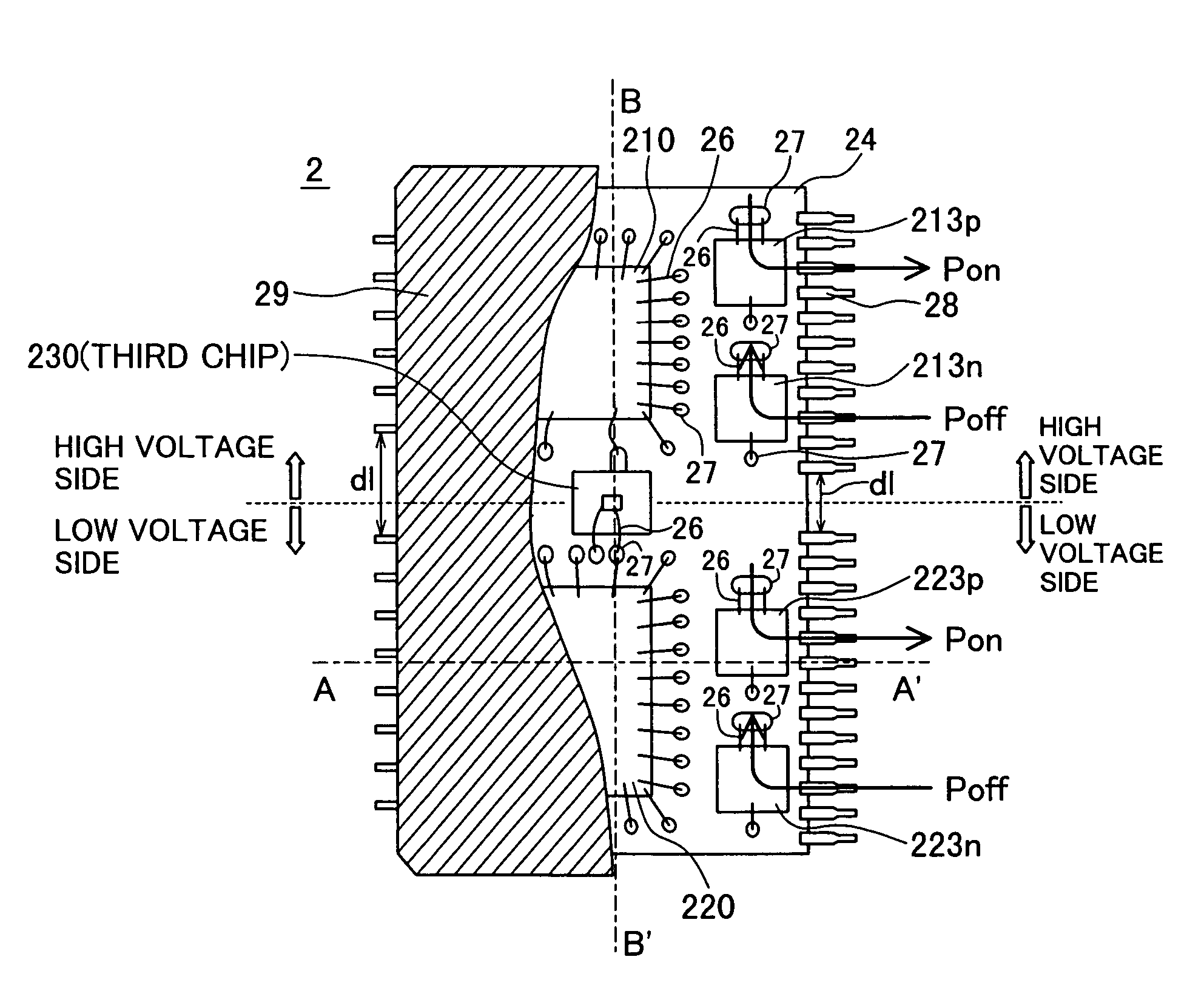
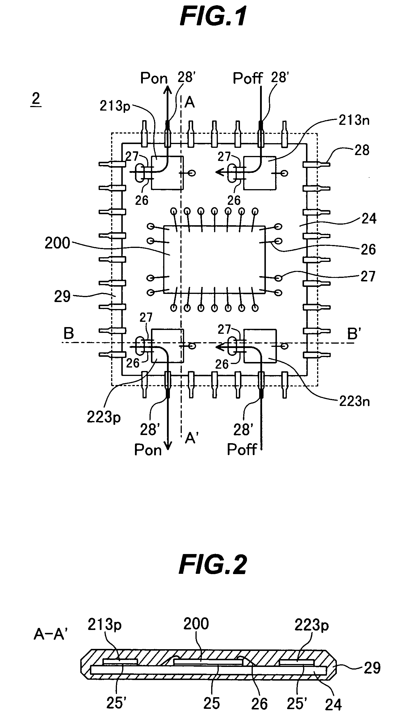
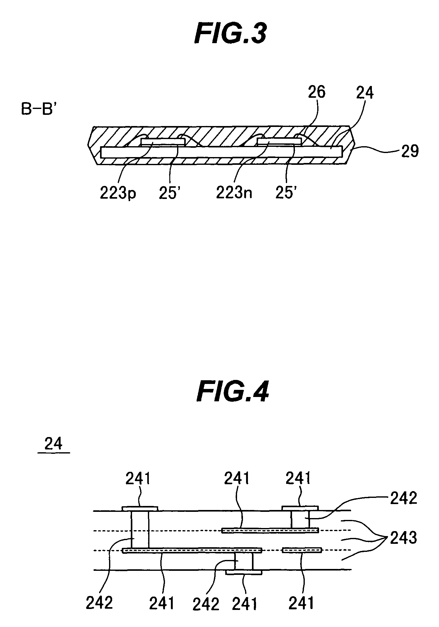
[0071]This embodiment is a modification of the first embodiment. In addition to the final output stage buffer sections 213, 223 being built in separate chips, the circuit elements constituting the level shift circuit 20 are also built in separate chips. Further, the high withstand voltage IC chip 200 is separated into a high voltage section and a low voltage section, which are built in separate chips. More specifically, in this embodiment, circuit elements c...

embodiment 3

[0083]A third embodiment of the present invention will be described with reference to FIGS. 14 through 18. FIGS. 14 through 16 show the construction of a driver IC of this embodiment. FIGS. 17 and 18 show the construction of an inverter of this embodiment. In the following, only the construction differing from that of the above-mentioned embodiments will be described and a description of the remaining similar construction is omitted.

[0084]This embodiment is an improved version of the second embodiment. The upper arm IC chip 210 and the lower arm IC chip 220 are each connected onto the isolation wiring board 24 by facedown (flip-chip) bonding with solder balls 261 (in BGA (Ball Grid Array)). With this embodiment thus constructed, since the wires and the bonding pads are omitted, the occupancy area of the upper arm IC chip 210 and the lower arm IC chip 220 is reduced. Also, with this embodiment, such a reduction of the occupancy area enables the passive parts 5 for filtering, which ar...

embodiment 4

[0091]A drive system of this embodiment, shown in FIG. 19, comprises a drive circuit 402, a drive circuit 403, resistances 404 and 405 for connecting the drive circuit 402 and the drive circuit 403 to the gate of the IGBT 32H (32L), a gate power supply V, a control circuit 406 for controlling the operations of the drive circuits, a slope detecting circuit 407, and a timer circuit 410 for transferring an output of the slope detecting circuit 407 to a later stage after the lapse of a preset time.

[0092]The slope detecting circuit 407 comprises a change rate detecting circuit 408 for detecting a time change rate of the gate voltage of the IGBT 32H (32L), and a waveform shaping circuit 409 for shaping an output waveform from the change rate detecting circuit 408.

[0093]If an output signal of the change rate detecting circuit 408 is at a level sufficient for being transferred to the stage downstream of the slope detecting circuit 407, the waveform shaping circuit 409 may be dispensed with....


PUM


Abstract

An integrated circuit for driving a semiconductor device, which is adaptable for demands, such as a higher output (larger current), a higher voltage, and a smaller loss, and has a small size, is produced at a low cost, and has high reliability. A power converter including such an integrated circuit is also provided. Circuit elements constituting a drive section of an upper arm drive circuit 212, a level shift circuit 20 including a current sensing circuit 210, a drive section of a lower arm drive circuit 222, and a drive signal processing circuit 224 are integrated and built in one high withstand voltage IC chip 200. Circuit elements constituting a final output stage buffer section 213 of the upper arm drive circuit 212 are built in a vertical p-channel MOS-FET chip 213p and a vertical n-channel MOS-FET chip 213n. Circuit elements constituting a final output stage buffer section 223 of the lower arm drive circuit 222 are built in a vertical p-channel MOS-FET chip 223p and a vertical n-channel MOS-FET chip 223n. Thus, a driver IC 2 is fabricated.

Description

TECHNICAL FIELD[0001]The present invention relates to an integrated circuit for driving semiconductor device, and a power converter including such an integrated circuit.BACKGROUND ART[0002]A driver circuit for driving a semiconductor device is employed in all types of electric equipment and electronic equipment. As one example of the equipment, there is a power converter, e.g., an inverter for converting DC power supplied from a power supply to AC power, and supplying the AC power to an electric motor as a load. The driver circuit is made up of a plurality of circuit elements constituting a plurality of circuits, e.g., a circuit for generating a drive signal in accordance with an external command and a circuit for supplying drive power to the semiconductor device in accordance with the drive signal.[0003]Hitherto, known driver circuits have been described, for example, in JP,A 5-316755 and “Hitachi High Withstand Voltage Monolithic IC Data Book-Motor Driving IC Series”, by Hitachi L...

Claims


Application Information

Patent Timeline
Patent Type & Authority Patents(United States)
IPC IPC(8): H01L23/34H02M1/08
CPCH01L24/49H01L25/072H01L25/162H02M1/08H01L24/45H01L2224/45124H01L2224/45144H01L2224/48091H01L2224/48137H01L2224/48227H01L2224/48247H01L2224/49111H01L2224/49171H01L2224/73204H01L2924/01004H01L2924/01005H01L2924/01006H01L2924/01013H01L2924/01014H01L2924/01015H01L2924/01018H01L2924/01027H01L2924/01028H01L2924/01029H01L2924/01033H01L2924/01039H01L2924/01042H01L2924/01046H01L2924/01047H01L2924/01051H01L2924/01074H01L2924/01075H01L2924/01078H01L2924/01079H01L2924/01082H01L2924/01088H01L2924/09701H01L2924/13091H01L2924/14H01L2924/19041H01L2924/19043H01L2924/19105H01L2924/30105H01L2924/30107H01L2924/01019H01L2924/01023H01L2924/01037H01L2924/014H01L2224/73265H01L2224/16225H01L2224/32225H01L2224/48472H01L2224/49175H01L2924/19107H01L2924/13055H01L2924/1306H01L2924/1305H01L2924/00014H01L2924/00H01L2224/48139H01L2224/45015H01L2924/181H01L24/48H01L2924/00012
Inventor TAKAHASHI, YOSHIMASASAKURAI, NAOKIYURA, MASASHIIWAMURA, MASAHIROMORI, MUTSUHIRO
Owner HITACHI LTD
Learn More