
Method of manufacturing active matrix array structure

a technology of active matrix array and manufacturing method, which is applied in the direction of basic electric elements, electrical apparatus, semiconductor devices, etc., can solve the problems of difficult costing down of manufacturing process, and achieve the effect of increasing the display aperture ratio of liquid crystal display panels

Active Publication Date: 2010-07-13
AU OPTRONICS CORP
View PDF9 Cites 3 Cited by
  • Summary
  • Abstract
  • Description
  • Claims
  • Application Information

AI Technical Summary

Benefits of technology

[0011]In view of the foregoing, the present invention provides an active matrix array structure, which is applicable in a liquid crystal display panel to increase the display aperture ratio of the liquid crystal display panel.
[0012]The present invention also provides a method for fabricating an active matrix array structure, in which the manufacturing cost required in fabricating an active matrix array structure is reduced.
[0031]The present invention applies three photomasking processes to fabricate an active matrix array structure having an overcoat layer. Hence, the fabrication cost is greatly reduced due to a reduction of the number of photomasks being used. Moreover, in the active matrix array structure of the present invention, the disposition of the overcoat layer mitigates the parasitic capacitor between the pixel electrodes and the data lines. Accordingly, the transparent conductive layer is partially overlapped with the date lines to increase the display aperture ratio of the active matrix array structure.

Problems solved by technology

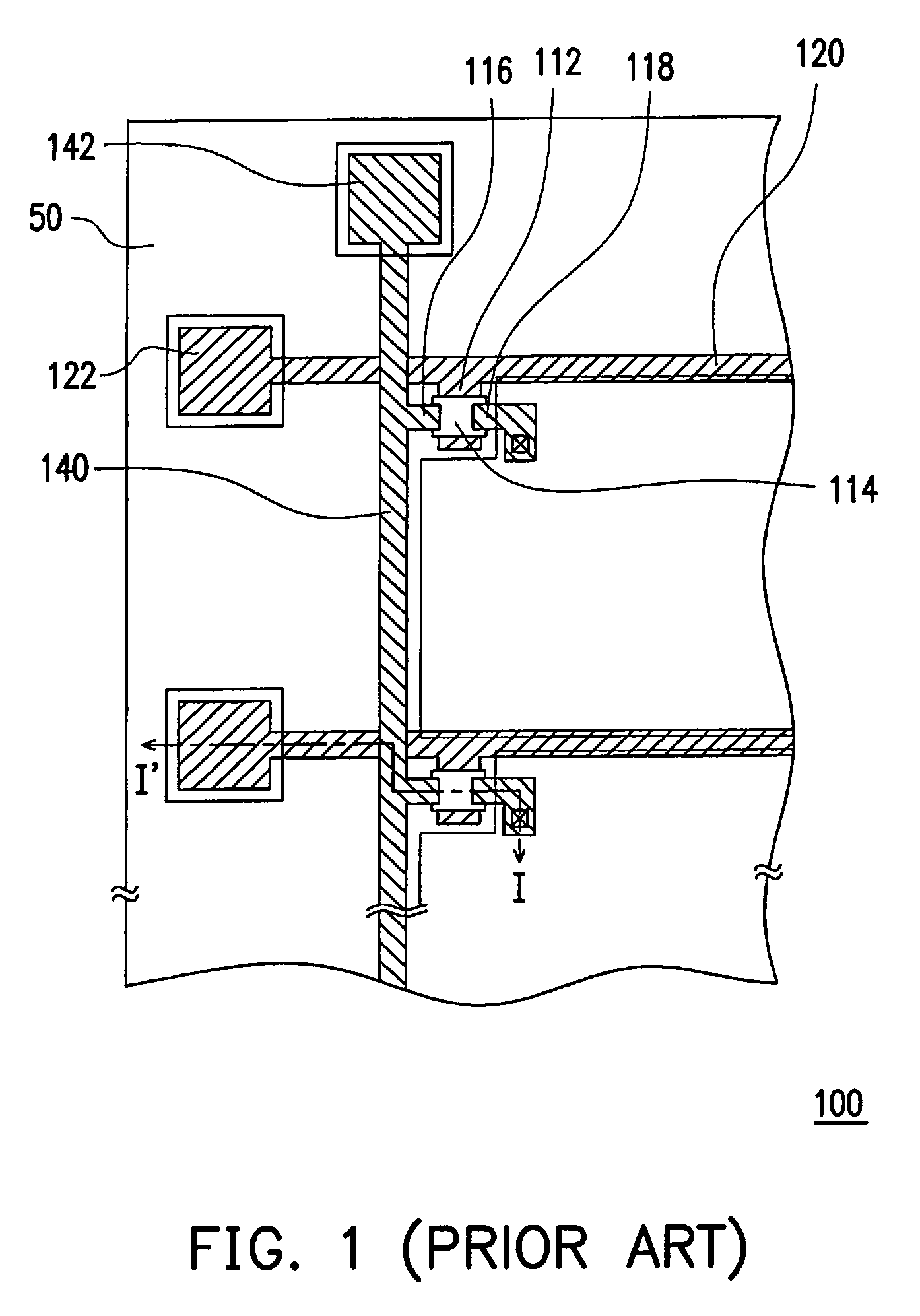
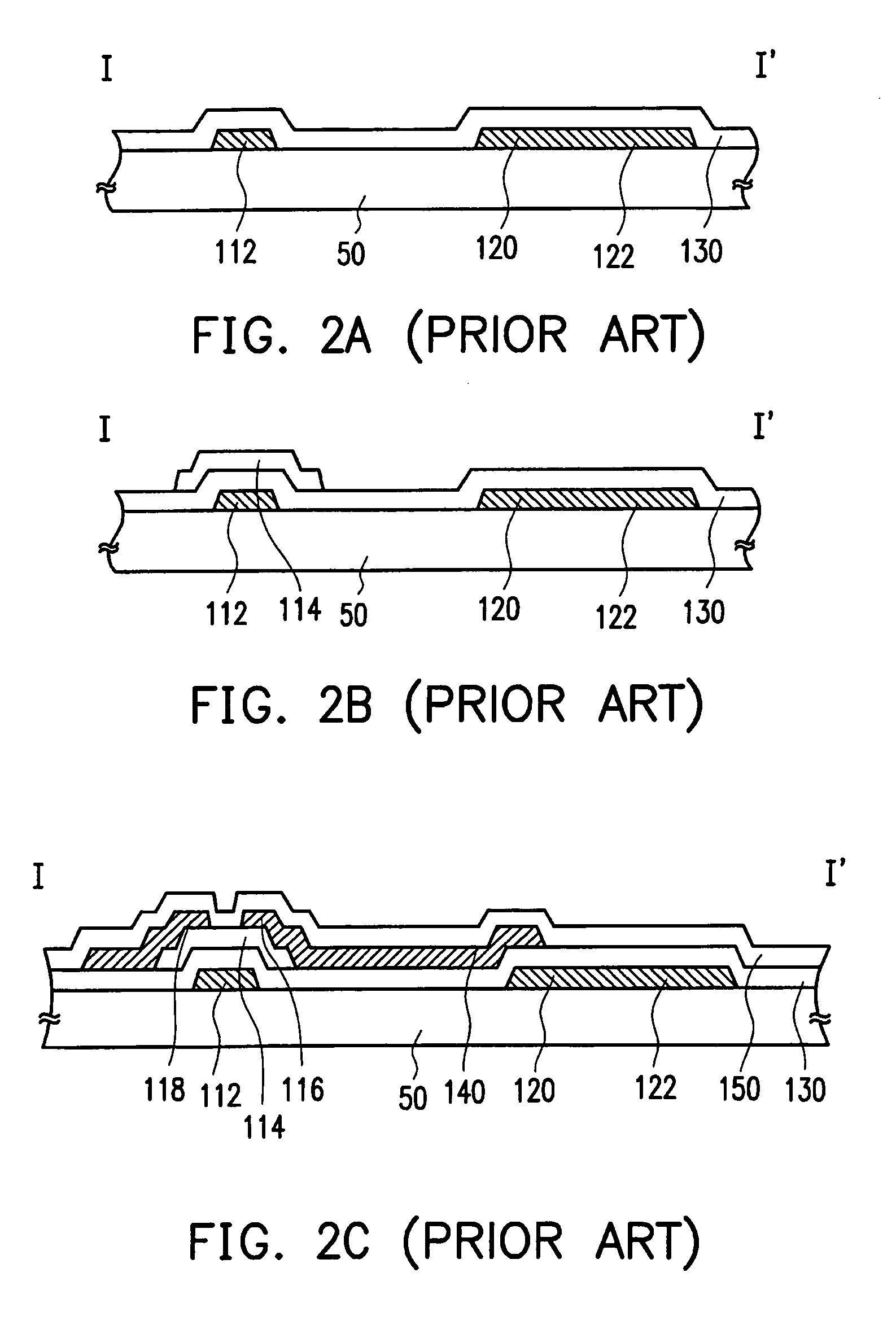
However, with the application of five photomasks, the costing down of the manufacturing process becomes difficult.

Method used


Image

  • Method of manufacturing active matrix array structure
  • Method of manufacturing active matrix array structure
  • Method of manufacturing active matrix array structure

Examples


first embodiment

[0059]FIG. 3 is a top view showing the first photomasking process of the active matrix array structure according to a first embodiment of the invention. FIGS. 4A to 4D are cross sectional views of FIG. 3 along the cutting lines AA′, BB′ CC′ and DD″, respectively. Referring to FIGS. 3 and 4A to 4D, the fabrication of an active matrix array structure of this embodiment of the invention includes forming a first conductive layer (not shown) on a substrate 300, and patterning the first conductive layer (not shown) by performing a first photomasking process to form a first patterned conductive layer 310. The first patterned conductive layer 310 includes a plurality of scan lines 312, a plurality of gates 314 and a plurality of scan contact pads 316, and the scan lines 312 are connected with the gates 314 and the scan contact pads 316.

[0060]In this embodiment, the first patterned conductive layer 310 includes, for example, a multi-layer of metal stacked layer structure constructed with a f...

second embodiment

[0081]FIG. 14 is a schematic diagram illustrating an active matrix array structure according to a second embodiment of the present invention. FIGS. 15A to 15D are cross-sectional views of FIG. 14 along the cutting lines AA′, BB′ CC′ and DD′. Referring to FIGS. 14 and 15A to 15D, the active matrix array structure 600 and the active matrix array structure 380 in the first embodiment are substantially similar. The active matrix array structure 600 further includes a patterned passivation layer 680 configured between the patterned overcoat layer 360 and the substrate 300. Moreover, in this embodiment, the metal stacked layer structure that forms the gate 314, the scan line 312 and the scan pad 316 includes, for example, a stacked structure of aluminum and molybdenum or a molybdenum / aluminum / molybdenum three-layered stacked structure. Concurrently, the metal structure that forms the date lines 332, the source electrodes 334, the drain electrodes 336 and the data contact pads 338 includes...

third embodiment

[0085]FIG. 16 is a schematic diagram illustrating an active matrix array structure according to a third embodiment of the present invention. FIGS. 17A to 17D are cross-sectional views of FIG. 16 along the cutting lines AA′, BB′ CC′ and DD′. Referring to FIG. 16 and FIGS. 17A to 17D, a first patterned conductive layer 702 is formed on a substrate 700. The first patterned conductive layer 702 is a stacked layer structure that includes a first aluminum metal layer and a first molybdenum layer. During the first photomasking process, a normal photomask is used to perform photolithograph and etching processes in forming a first patterned conductive layer 702.

[0086]Moreover, the first patterned conductive layer 702 includes a scan line 704, a scan contact pad 706, a gate 708, a capacitor lower electrode 710 and an auxiliary pad 712. The scan line 704, the scan contact pad 706, the gate 708 and the capacitor lower electrode 710 are electrically connected. Moreover, the scan contact pad 706 ...


PUM


Abstract

An active matrix array structure, disposed on a substrate, includes a first patterned conductive layer, a patterned gate insulating layer, a patterned semiconductor layer, a second patterned conductive layer, a patterned overcoat layer and a transparent conductive layer. The patterned gate insulating layer has first openings that expose a part of the first patterned conductive layer. The patterned semiconductor layer is disposed on the patterned gate insulating layer. The second patterned conductive layer is disposed on the patterned semiconductor layer. The patterned overcoat layer has second openings that expose a part of the first patterned conductive layer and a part of the second patterned conductive layer. The transparent conductive layer is completely disposed on the substrate. The transparent conductive layer disposed in the first openings and the second openings is broken off at a position that is in between the substrate and the patterned overcoat layer.

Description

CROSS-REFERENCE TO RELATED APPLICATION[0001]This application claims the priority benefit of Taiwan application serial no. 97100663, filed on Jan. 8, 2008. The entirety the above-mentioned patent application is hereby incorporated by reference herein and made a part of specification.BACKGROUND OF THE INVENTION[0002]1. Field of Invention[0003]The present invention relates to an active matrix array structure and a manufacturing method thereof. More particularly, the present invention relates to an active matrix array structure with an overcoat layer and a manufacturing method thereof.[0004]2. Description of Related Art[0005]A thin film transistor liquid crystal display panel (TFT LCD panel) is constructed with an active matrix array structure, a color filter array structure and a liquid crystal layer. The active matrix array structure is configured with a plurality of arrays in rows and columns of active devices, i.e. the thin film transistors (TFT), and a pixel electrode corresponding...

Claims


Application Information

Patent Timeline
Patent Type & Authority Patents(United States)
IPC IPC(8): H01L21/00
CPCH01L27/124H01L27/1288H01L27/1248
Inventor YU, WEI-SHENGFANG, KUO-LUNGLIN, HSIANG-LINTSENG, HSIEN-CHIEHLIN, HAN-TU
Owner AU OPTRONICS CORP
Learn More