Method of manufacturing clad board for forming circuitry, clad board and core board for clad board
a manufacturing method and technology for forming circuits, applied in the field of manufacturing a clad board for forming circuitry, a clad board, and a core board for clad boards, can solve the problems of short-circuit or lower insulating reliability between wiring, and problems that increase at a higher density of wiring patterns, so as to prevent short-circuits and reduce insulating reliability, the effect of increasing the yield rate of circuit boards
- Summary
- Abstract
- Description
- Claims
- Application Information
AI Technical Summary
Benefits of technology
Problems solved by technology
Method used
Image

Examples
exemplary embodiment 1
[0022]A first exemplary embodiment of the present invention will be described with reference to FIG. 1A to FIG. 4F. FIG. 4A to FIG. 4F are sectional views illustrating a method of manufacturing a clad board for forming circuitry in accordance with the first exemplary embodiment. The manufacturing method includes a releasing-film-sticking step, a hole-forming step, conductive-paste-filling step, peeling-off step, heat-and-pressure-applying step, and circuit-forming step.
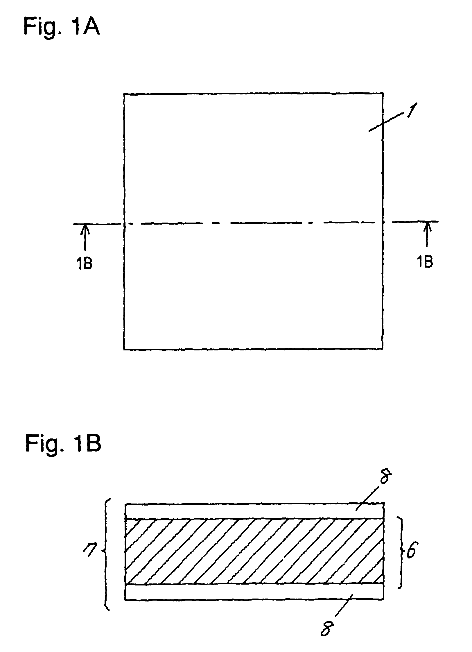
[0023]As shown in FIG. 1A and FIG. 1B, pre-preg sheet 1 is a composite material including impregnated resin 7 (e.g. thermosetting resin such as epoxy resin) and non-woven fabric 6 of fiber sheet such as aromatic polyamide fiber (aramid fiber). Impregnated resin 7 is not completely cured but includes a semi-cured portion, i.e., impregnated resin 7 is in B-stage.
[0024]Releasing film 2 shown in FIG. 4A is formed of polymer film such as polyethylene terephthalate (PET) of 20 μm thickness, having a silicon-based releasing ...
exemplary embodiment 2
[0037]A manufacturing method in accordance with a second exemplary embodiment is basically the same as that of the first embodiment, and detailed description is thus omitted here. Features only in the second embodiment will be described.
[0038]Pre-preg sheet 1 is a composite material formed of thermosetting resin such as epoxy resin (hereinafter called impregnated resin 7) and non-woven fabric 6 of fabric sheet such as aromatic polyamide fiber (aramid fiber). Impregnated resin 7 is not completely cured but includes semi-cured portions, i.e., impregnated resin 7 is in B-stage.
[0039]Aramid fiber non-woven fabric 6 conventionally used for pre-preg sheet 1 has a density ranging from 500 to 700 kg / m3. When resin is impregnated into such non-woven fabric 6, the center section of fabric 6 tends to be impregnated. Therefore, resin is not fully enough impregnated around a surface, and fibers of fabric 6 may be thus exposed on the surface in parts as shown in FIG. 6A and FIG. 6B.
[0040]However,...
exemplary embodiment 3
[0048]A manufacturing method in accordance with a third exemplary embodiment is basically the same as that of the first embodiment, and detailed description is thus omitted here. Features only in the third embodiment will be demonstrated.
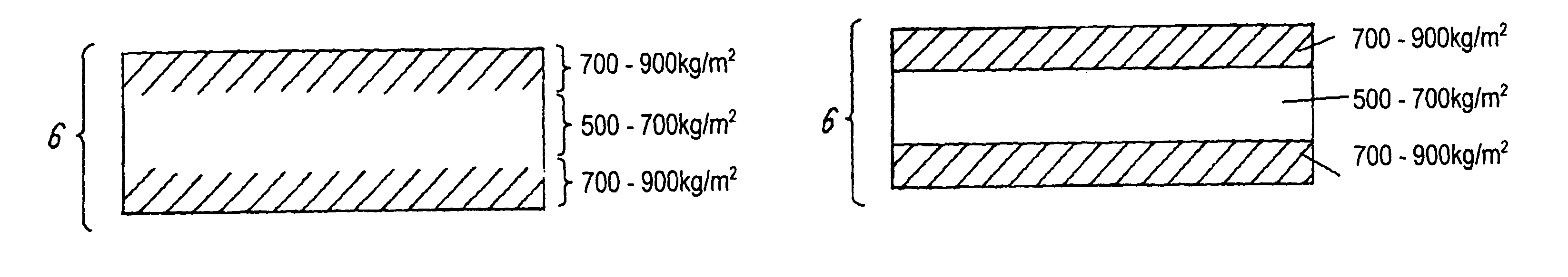
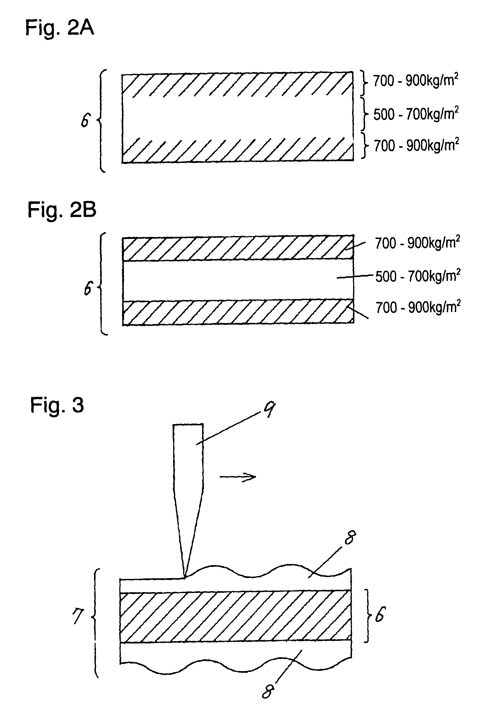
[0049]Aramid fiber non-woven fabric 6 used in the third embodiment has a density ranging from 700 to 1000 kg / m3 around a surface layer of both the faces of fabric 6 as shown in FIG. 2A. The density of the inside of fabric 6 is lower than that around the surface layer, and preferably ranges from 500 to 700 kg / m3.
[0050]If the density becomes lower than 500 kg / m3, a number of air-gaps in pre-preg sheet 1 increases. This makes conductive paste 4 tend to spread from inside of through holes 3 into pre-preg sheet 1 and the lowers its insulating reliability.
[0051]In pre-preg sheet 1 having the composition discussed above, resin is not impregnated well in the center section of aramid fiber non-woven fabric 6. Instead, much more resin component is attached ar...
PUM
| Property | Measurement | Unit |
|---|---|---|
| density | aaaaa | aaaaa |
| weight % | aaaaa | aaaaa |
| density | aaaaa | aaaaa |
Abstract
Description
Claims
Application Information
 - R&D
- Intellectual Property
- Life Sciences
- Materials
- Tech Scout
- Unparalleled Data Quality
- Higher Quality Content
- 60% Fewer Hallucinations
Browse by: Latest US Patents, China's latest patents, Technical Efficacy Thesaurus, Application Domain, Technology Topic, Popular Technical Reports.
© 2025 PatSnap. All rights reserved.Legal|Privacy policy|Modern Slavery Act Transparency Statement|Sitemap|About US| Contact US: help@patsnap.com