
Forward error correction (FEC) enabled photonic integrated circuit (PICs) chips with multiple signal channels

a technology of forward error correction and photonic integrated circuits, applied in the direction of transmission monitoring, instruments, semiconductor lasers, etc., can solve the problems of deteriorating channel signals, affecting the efficiency of optical communication networks, so as to improve yield, wide choice of design in channel count and/or channel spacing, and the effect of reducing the spacing

Active Publication Date: 2010-06-08
INFINERA CORP
View PDF18 Cites 70 Cited by
  • Summary
  • Abstract
  • Description
  • Claims
  • Application Information

AI Technical Summary

Benefits of technology

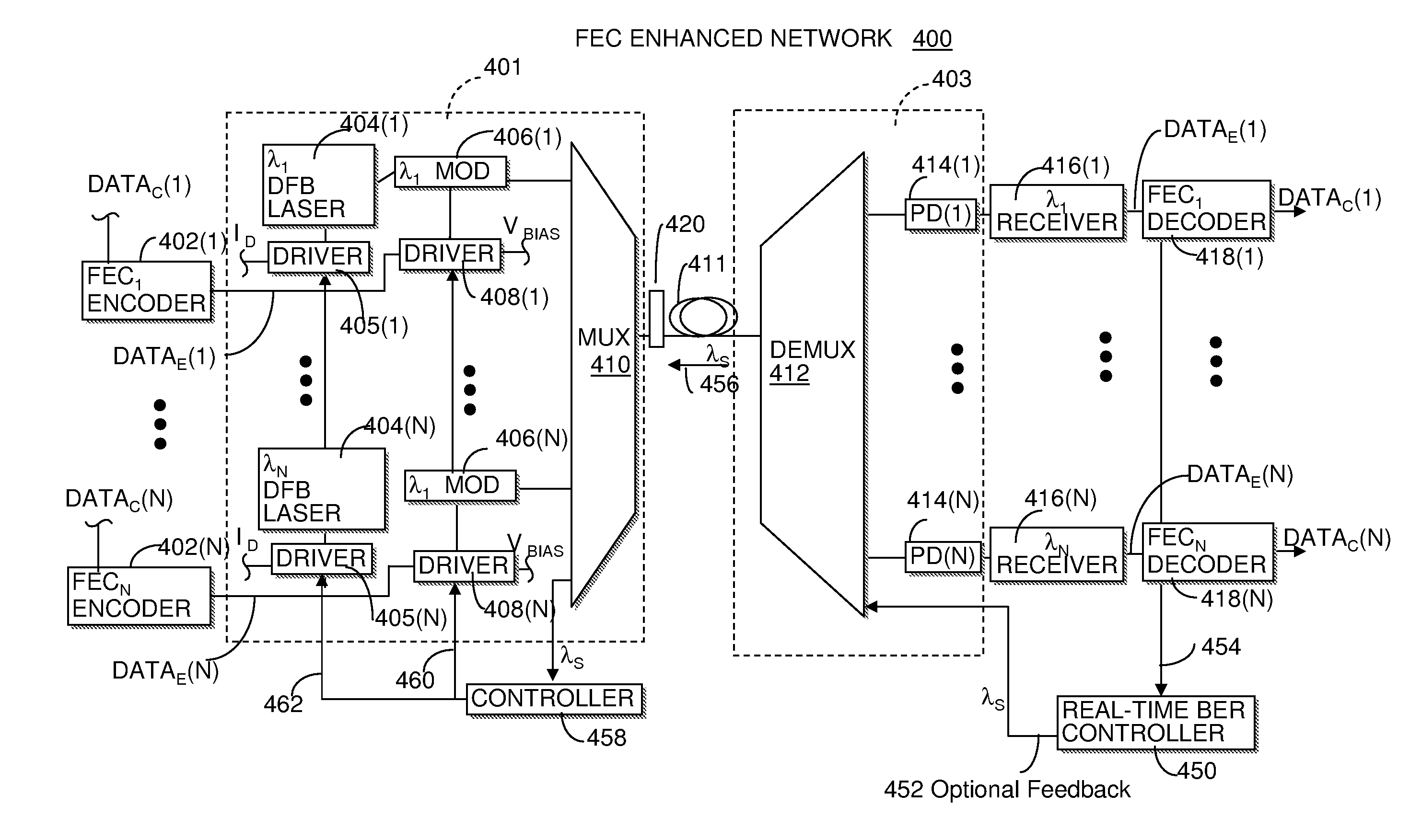
[0017]According to this invention, one way of combating the foregoing issues of signal distortion and deterioration in PICs and PLCs is to employ forward error correction (FEC) in combination with the PIC, in particular, a multi-channel PIC chip (TxPIC and / or RxPIC). Also, the operating parameter specification of a multi-channel PIC can be relaxed by utilizing FEC in combination with optical communication devices so as to improve yield on the multi-channel PIC chip Also, the operation windows of the active and / or passive elements on the multi-channel PICs can be made effectively wider thereby providing a wider choice of design in channel count and / or channel spacing. For example, the channel spacing can be made smaller thereby increasing the quantity of laser emission wavelength sources possible on a single multi-channel PIC chip. Alternatively, the channel spacing could be made wider, thereby allowing additional tolerances in the fabrication of the active and / or passive devices responsible for a targeted channel frequency. Such a multi-channel PIC chip, although having properties outside desired specifications for network operation, may still be acceptable to transmit distorted channel signals to an optical receiver if the generated optical channel signals also include FEC encoding which provides for compensation of numerous transmission penalties including penalties that arise from RIN, linewidth or SMSR degradation, or dispersion penalties, all of which may increase as the number of emission wavelengths, λ1, . . . , λN, increases in a multi-channel TxPIC.

Problems solved by technology

For example, four wave mixing (FWM) and amplified spontaneous emission (ASE) may become significant and deteriorate the channel signals.
Second, employing FEC provides a cost-performance tradeoff.
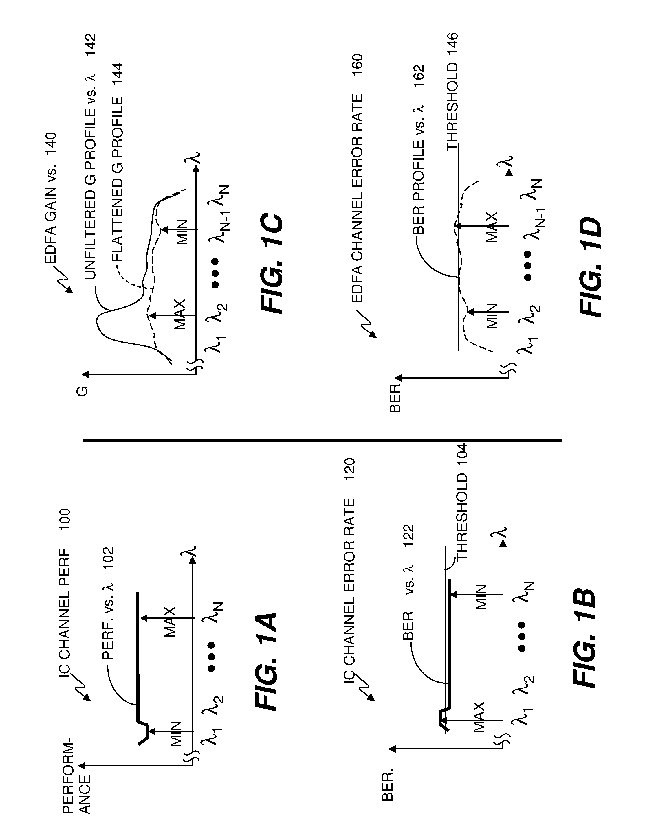
The deployment of multiple channels in a PIC results in compromised performance vis-à-vis each other.
For example, one trade-off might be degradation in laser performance across the array of laser sources, such as in the case of threshold current, spectral characteristics, and operational efficiency as well as increase in relative intensity noise (RIN).
Second, performance degradation across the transmission wavelength window may occur in the array of modulators.
It should be understood that placing a practical number of operable wavelengths on a TxPIC to achieve worthwhile integration results in a range of laser wavelengths within a modulator operating window that is inconsistent with techniques and approaches employed in the past and is a monumental task.
However, if an optical isolator is located immediately after a laser or modulator to protect those optical devices from noise and reflection then integrating then integrating them into a monolithic device would be difficult as materials used in an optical isolator include ferro magnetic magneto-optical material.
However, in the case of integrated arrays of lasers on a single chip, there is no luxury to mix and match because all of the optical signal sources are formed in large scale photonic integration in close relationship and, therefore, the performance of all the lasers in the array must be initially and successfully fabricated to desired specifications so that all of the integrated electro-optic elements on a PIC respectively meet the requisite assigned grid wavelength emission and operational specifications without unacceptable signal distortion deterioration if desirable yields of such photonic integrated circuits or PICs are to be realized.
Thus, as indicated previously, having the optical channel signals generated on a monolithic, large scale integration, multi-channel PIC chip have some attendant issues relative to providing acceptable BER levels at the optical receiver.
In particular, issues can arise from either the serial coupling of active / passive elements in a given channel (intrachannel) or the interaction between the active / passive elements from one channel to another (interchannel).
Because the signal channels are physically much closer to one another on a PIC having multiple channels, such as compared, for example, to the use of discrete modulated sources and discrete wavelength selective combiner, and because they are generally interconnected by low-loss waveguides and passive elements, there is an increase potential of signal distortion or deterioration due to, for example, channel crosstalk, RIN, SMSR, optical feedback channel noise, occasional wavelength hops.
Also, in connection with feedback channel noise, there is reflected feedback, such as optical feedback reflection from the wavelength selective combiner in the channel sources, which can also deteriorate channel signal quality.
Because of the failure of λN-1 to meet the threshold BER, the communication device responsible for the poor performance, e.g., a TxPIC and / or an RxPIC, may be unsuitable for field application, despite the satisfactory performance of the balance of the channels on the chip.
Many sources of noise and signal distortion arise in a communication network.
Channel noise and interference may arise from optical couplings, splices, taps, in-line amplifiers, compromised cladding, and other environmental influences.
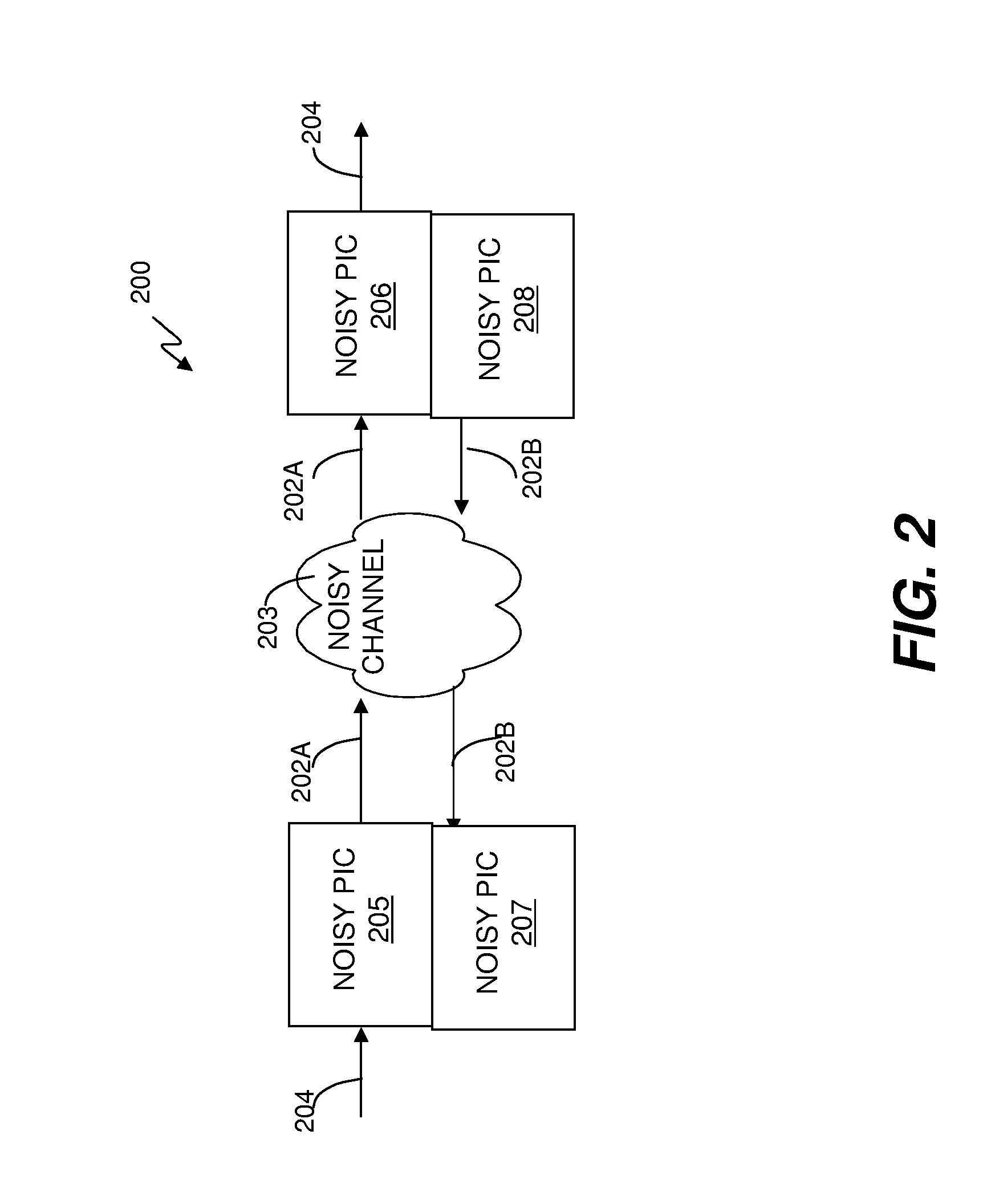
However if a noisy transmitter generates an unusually high amount of errors, it may consume the ability of a per-channel FEC to recover the data.

Method used


Image

  • Forward error correction (FEC) enabled photonic integrated circuit (PICs) chips with multiple signal channels
  • Forward error correction (FEC) enabled photonic integrated circuit (PICs) chips with multiple signal channels
  • Forward error correction (FEC) enabled photonic integrated circuit (PICs) chips with multiple signal channels

Examples


Embodiment Construction

[0030]Reference is now made to FIG. 4A of the present invention, as adapted from FIG. 70 of U.S. Pat. No. 7,116,851, supra. As shown in FIG. 4A, a forward error correction (FEC) enhanced optical transport network 400 shown as single direction transmission in a point-to-point optical transmission link including at least one multi-channel TxPIC 401 and at least one multi-channel RxPIC 403 in optical communication optical link 411. It should be understood that FEC enhanced network 400 can be bidirectional where multi-channel TxPIC 401 can also be a transceiver that includes a receiver, such as RxPIC 403 therein. In any application as a transmitter, receiver, or transceiver, the present invention is well suited to any combination and quantity of integrated or discrete transmitter and receiver components. For example, one communication system could use a transceiver with only a single integrated PIC pair (a TxPIC coupled to an RxPIC), while another system uses any combination of the two ...


PUM


Abstract

A forward error correction (FEC) communication device that includes a transmitter photonic integrated circuit (TxPIC) or a receiver photonic integrated circuit (RxPIC) and a FEC device for FEC coding at least one channel with a first error rate and at least one additional channel with a second error rate, wherein the first error rate is greater than the second error rate. The TxPIC chip is a monolithic multi-channel chip having an array of modulated sources integrated on the chip, each operating at a different wavelength, wherein at least one of the modulated sources is modulated with a respective FEC encoded signal. The TxPIC also includes an integrated wavelength selective combiner for combining the channels for transport over an optical link.

Description

REFERENCE TO RELATED APPLICATION[0001]This application is a continuation-in-part of parent U.S. Pat. No. 7,116,851 entitled An Optical Signal Receiver Photonic Integrated Circuit (RxPIC), AN ASSOCIATED OPTICAL SIGNAL TRANSMITTER PHOTONIC INTEGRATED CIRCUIT (TXPIC) AND AN OPTICAL TRANSPORT NETWORK UTILIZING THESE CIRCUITS, issued Oct. 3, 2006; and is a continuation in part of Ser. No. 10 / 712,732, entitled METHOD AND APPARATUS FOR DEPLOYING FORWARD ERROR CORRECTION (FEC) IN OPTICAL TRANSMISSION NETWORKS AND THE DEPLOYMENT OF PHOTONIC INTEGRATED CIRCUIT (PIC) CHIPS WITH THE SAME, filed Nov. 12, 2003, both owned by the common assignee herein, which applications are incorporated herein by their reference. This application claims priority to U.S. provisional application Ser. No. 60 / 748,989, filed Dec. 9, 2005, owned by the common assignee herein, which application is incorporated herein by its reference.BACKGROUND OF THE INVENTION[0002]1. Field of the Invention[0003]This invention relates...

Claims


Application Information

Patent Timeline
IPC IPC(8): H04B10/00H04B10/04H04B10/08
CPCB82Y20/00H01S5/0265H01S5/22H01S5/4025H01S5/4031H04B10/25H04B10/2914H04B10/50H04B10/675H04J14/02H04J14/0279H01S5/026H01S5/0264H01S5/0268H01S5/06256H01S5/06258H01S5/0683H01S5/1228H01S5/2077H01S5/3408H01S5/4087H01S5/50G02B6/12021
Inventor WELCH, DAVID F.PERKINS, DREW D.KISH, JR., FRED A.CHIANG, TING-KUANG
Owner INFINERA CORP
Learn More