Field effect transistor having nitride semiconductor layer

a field effect transistor and semiconductor layer technology, applied in the field of field effect transistors, can solve the problems of disadvantageous increase parasitic resistance, and achieve the effects of suppressing the increase of parasitic resistance, high crystallinity, and suppressing the degradation of the inalgan layer otherwise caused in annealing

Active Publication Date: 2010-05-11
PANASONIC CORP
View PDF2 Cites 4 Cited by
  • Summary
  • Abstract
  • Description
  • Claims
  • Application Information

AI Technical Summary

Benefits of technology

[0011]In consideration of the aforementioned conventional disadvantages, an object of the invention is, in a heterojunction field effect transistor, suppressing increase of parasitic resistance on a hetero interface so as to improve transistor characteristics such as high-frequency characteristics.
[0046]As described so far, when the field effect transistor and the fabrication method for the same of this invention are applied to a high-frequency high-output-power transistor, increase of parasitic resistance on a hetero interface between a compound semiconductor layer and an InAlGaN layer can be suppressed, so as to largely improve the device characteristics such as high-frequency characteristics.

Problems solved by technology

In the conventional field effect transistor disclosed in Patent Document 1, however, there is a large potential barrier on the InAlGaN / AlGaN interface as shown in FIG. 9C, which disadvantageously increases parasitic resistance.

Method used


Image

  • Field effect transistor having nitride semiconductor layer
  • Field effect transistor having nitride semiconductor layer
  • Field effect transistor having nitride semiconductor layer

Examples


embodiment 1

Modification of Embodiment 1

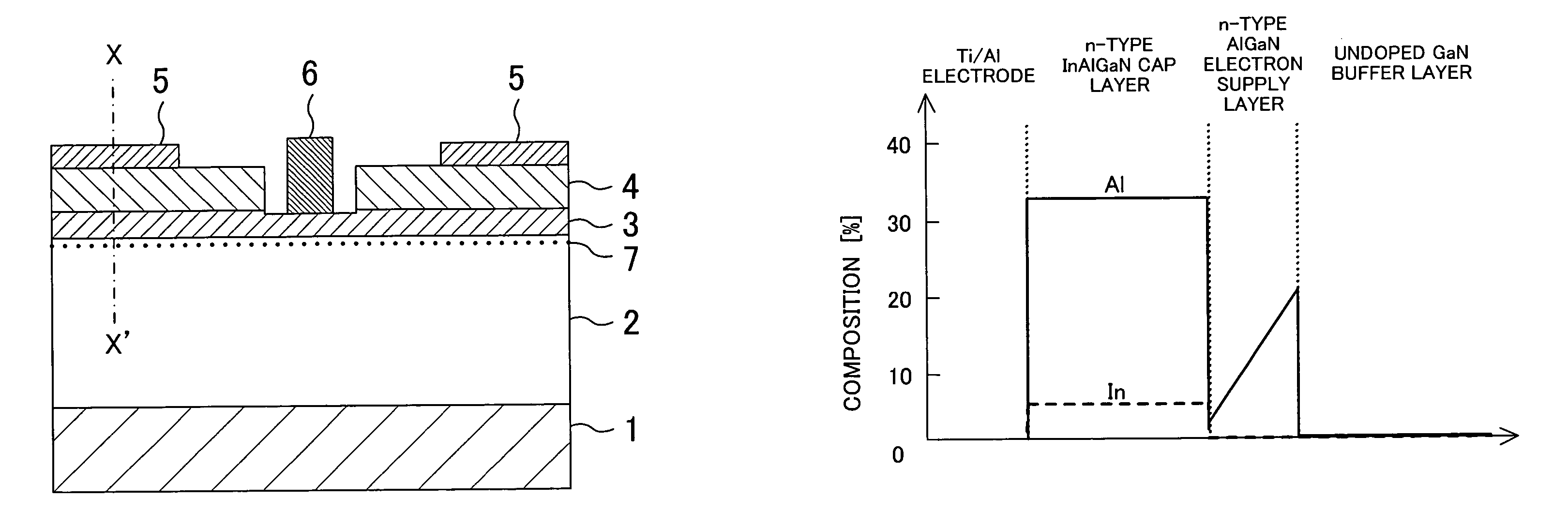
[0088]A method for fabricating a field effect transistor according to a modification of Embodiment 1 of the invention will now be described with reference to the accompanying drawings. In the fabrication method of this modification, the field effect transistor of Embodiment 1 shown in FIG. 1A is fabricated.

[0089]FIGS. 6A through 6F are cross-sectional views for showing procedures in the method for fabricating the field effect transistor of this modification. Although the recess corresponding to a gate electrode forming region is formed by etching the n-type InAlGaN cap layer 4 in the procedure shown in FIG. 5B in Embodiment 1, the recess is formed by regrowing the n-type InAlGaN cap layer 4 after masking a gate electrode forming region on the n-type AlGaN electron supply layer 3 as described below in this modification.

[0090]First, as shown in FIG. 6A, an undoped GaN buffer layer 2 and an n-type AlGaN electron supply layer 3 are successively formed on the ...

embodiment 2

[0098]A field effect transistor and a method for fabricating the same according to Embodiment 2 of the invention will now be described with reference to the accompanying drawings.

[0099]FIG. 7 is a cross-sectional view of the field effect transistor of this embodiment. In FIG. 7, like reference numerals are used to refer to like elements used in Embodiment 1 shown in FIG. 1A. Embodiment 2 is different from Embodiment 1 in the following points as described below: Directly below an n-type InAlGaN cap layer 4, a multilayered film including at least one cycle of another InAlGaN layer and an AlGaN layer alternately stacked is provided; and an n-type AlGaN electron supply layer 3 (in which the Al composition is changed along the thickness direction as in Embodiment 1) is provided with a delta dope layer (i.e., a region including an impurity for providing the conductivity type to the n-type AlGaN electron supply layer 3 so as to cause a pulse-shaped profile along a direction vertical to the...


PUM


Abstract

A field effect transistor includes a nitride semiconductor layer; an InxAlyGa1-x-yN layer (wherein 0<x<1, 0<y<1 and 0<x+y<1) formed on the nitride semiconductor layer; and a source electrode and a drain electrode formed on and in contact with the InxAlyGa1-x-yN layer. The lower ends of the conduction bands of the nitride semiconductor layer and the InxAlyGa1-x-yN layer are substantially continuous on the interface therebetween.

Description

BACKGROUND OF THE INVENTION[0001]The present invention relates to a field effect transistor usable as a high-frequency high-output-power transistor and a method for fabricating the same.[0002]A group III-V nitride compound semiconductor typified by GaN (represented by a general formula, InxAlyGa1-x-yN (wherein 0≦x≦1 and 0≦y≦1) hereinafter referred to as InAlGaN) is regarded as a promising material for a high-frequency high-output-power electronic device because it has a wide band gap (of, for example, 3.4 eV at room temperature in GaN), a very large breakdown electric field and very high saturated electronic velocity. In particular, in a hetero junction structure obtained by stacking an AlGaN film on a GaN film (hereinafter referred to as an AlGaN / GaN hetero structure), electrons are stored in a high concentration in the vicinity of the hetero junction interface within the GaN film owing to a strong polarization electric field formed on the (0001) plane, so as to generate what is ca...

Claims


Application Information

Patent Timeline
Patent Type & Authority Patents(United States)
IPC IPC(8): H01L31/072H01L31/0328H01L31/0336H01L31/109
CPCH01L29/7787H01L29/365H01L29/2003
Inventor NAKAZAWA, SATOSHIUEDA, TETSUZOTANAKA, TSUYOSHI
Owner PANASONIC CORP
Why Eureka
Try Eureka