Microelectromechanical tunable inductor

a micro-electromechanical and inductor technology, applied in the field of micro-electromechanical devices, can solve the problems of large losses, prohibitive size, and significant parasitic effects, and achieve the effect of reducing the ac resistance of the coil

Active Publication Date: 2010-05-04
NAT TECH & ENG SOLUTIONS OF SANDIA LLC
View PDF16 Cites 17 Cited by
  • Summary
  • Abstract
  • Description
  • Claims
  • Application Information

AI Technical Summary

Benefits of technology

[0012]The coiling in the tunable inductor is due to a layer of a compressively-stressed material (e.g. silicon dioxide) and a layer of a tensile-stressed material (e.g. silicon nitride) which are laminated together to form the coils. In some embodiments of the present invention, each coil in the tunable inductor can have a shape which is tapered or stepped with distance from the first end to the second end. This is useful for forming the coils without tangling, and also to provide an inductance L which varies proportionately to an applied voltage V. In other embodiments of the present invention, the tunable inductor can have coils with a lattice structure, or with a density of etch-release holes that varies with distance from the first end to the second end.

Problems solved by technology

The on-chip integration of relatively high-Q fixed and variable inductors with silicon IC technology, however, has been problematic due to the parasitic effects of low-conductivity metallization as well as lossy substrate interactions.
However, drawbacks of the off-chip inductors include significant parasitic effects, prohibitive size, and large losses due to board-level flip-chip and / or surface-mount interconnections.
Inductors with disk-shaped coils wound about an axis which is substantially perpendicular to an underlying semiconductor substrate are lossy due to eddy currents induced in the closely underlying substrate, and also due skin effects which restrict an alternating current (AC) in the coil to a small skin depth at the edge of the coil thereby substantially increasing the AC resistance of the coil.

Method used


Image

  • Microelectromechanical tunable inductor
  • Microelectromechanical tunable inductor
  • Microelectromechanical tunable inductor

Examples


Embodiment Construction

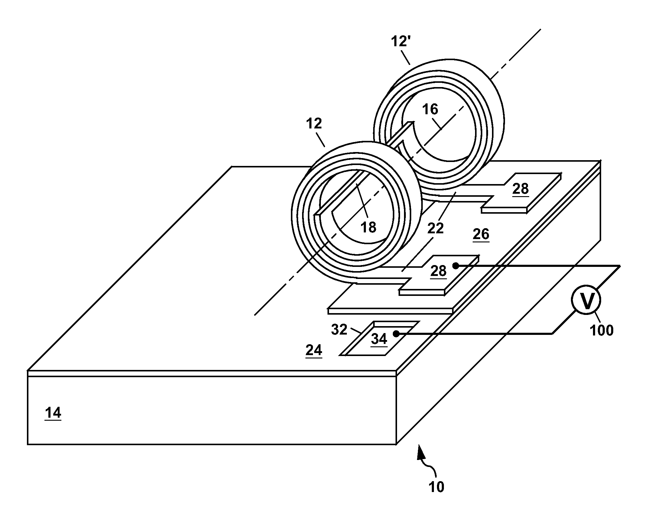
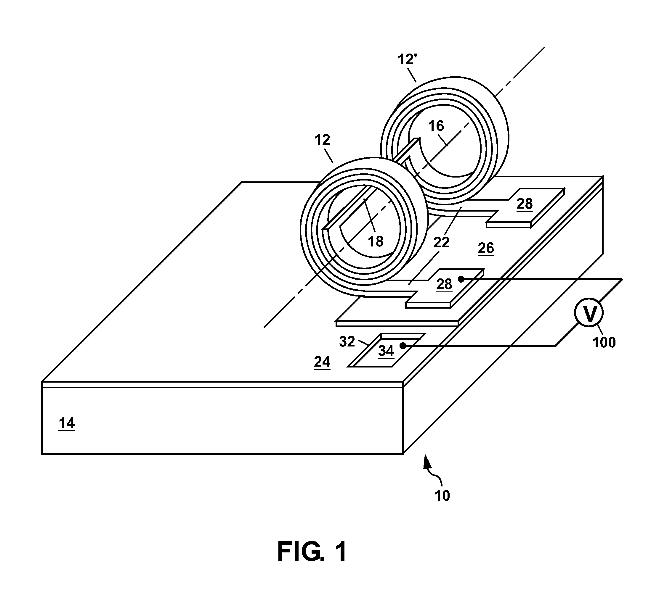
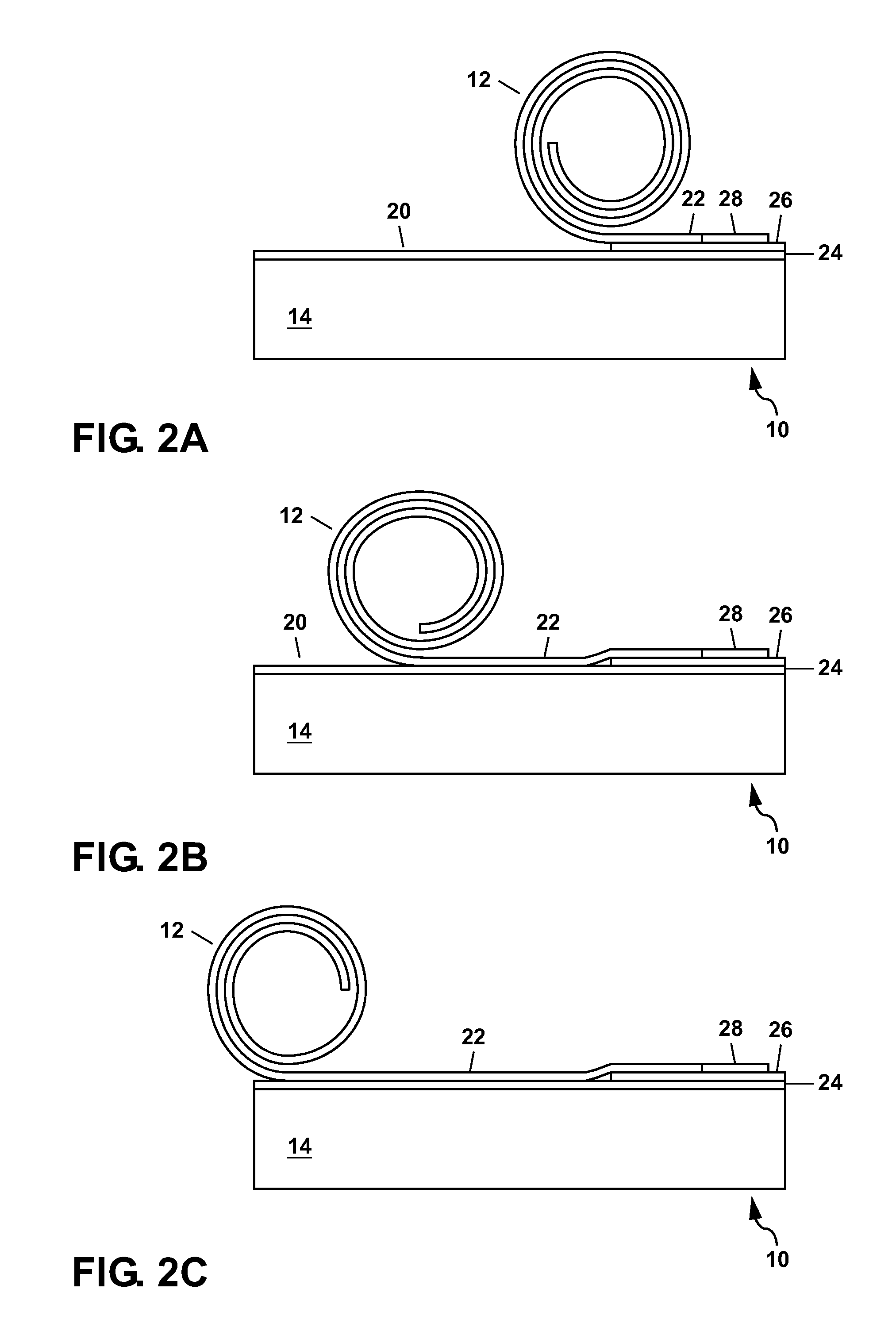
[0032]FIG. 1 shows a schematic perspective view of a first example of a tunable inductor 10 according to the present invention. In FIG. 1, the tunable inductor 10 is a microelectromechanical (MEM) device which comprises a pair of coils 12 and 12′ that are of substantially the same size and arranged side by side on a supporting substrate 14. The coils 12 and 12′ are also oriented substantially parallel to each other and comprise a plurality of turns. Each coil 12 and 12′ is formed from an elongate member (see FIGS. 5A-5D) which coils up about a central axis 16 which is oriented substantially parallel to the substrate 14 as shown in FIG. 1. A first end of each coil 12 and 12′ is anchored to the substrate 14, and a second end of each coil 12 and 12′ is used to connect the pair of coils 12 and 12′ together via a bridge 18 which is suspended above the substrate 14. The second end is also referred to herein as an unanchored end.

[0033]A first electrode in this example of the present invent...


PUM


Abstract

A microelectromechanical tunable inductor is formed from a pair of substantially-identically-sized coils arranged side by side and coiled up about a central axis which is parallel to a supporting substrate. An in-plane stress gradient is responsible for coiling up the coils which. The inductance provided by the tunable inductor can be electrostatically changed either continuously or in discrete steps using electrodes on the substrate and on each coil. The tunable inductor can be formed with processes which are compatible with conventional IC fabrication so that, in some cases, the tunable inductor can be formed on a semiconductor substrate alongside or on top of an IC.

Description

GOVERNMENT RIGHTS[0001]This invention was made with Government support under Contract No. DE-AC04-94AL85000 awarded by the U.S. Department of Energy. The Government has certain rights in the invention.FIELD OF THE INVENTION[0002]The present invention relates in general to microelectromechanical devices, and in particular to a tunable inductor which can be electrostatically tuned to change its inductance.BACKGROUND OF THE INVENTION[0003]In the radio frequency (RF) and microwave technology domain there is a need to integrate passive components including inductors, capacitors, switches and filters on an integrated circuit (IC) chip to lower device size and manufacturing cost and to improve performance and reliability. The integration of these passive devices into an RF IC will provide high value for such applications as voltage-controlled-oscillator (VCO), phase-locked-loop (PLL) and other RF functionality required for advanced telecom systems.[0004]Efforts have been focused on improvi...

Claims


Application Information

Patent Timeline
IPC IPC(8): H01F27/29H01F21/04H01F5/00H01G5/00H01H57/00H02N1/00
CPCH01F21/04H01F21/005
Inventor STALFORD, HAROLD L.HIETALA, VINCENT M.FLEMING, JAMES G.FLEMING, LEGAL REPRESENTATIVE, CAROL
Owner NAT TECH & ENG SOLUTIONS OF SANDIA LLC
Why Eureka
Try Eureka