Sensor device and production method therefor
a technology of sensor and production method, applied in the direction of acceleration measurement using interia force, semiconductor/solid-state device testing/measurement, instruments, etc., can solve problems such as sensor characteristics that vary, and achieve the effect of small variations in sensor characteristics
- Summary
- Abstract
- Description
- Claims
- Application Information
AI Technical Summary
Benefits of technology
Problems solved by technology
Method used
Image
Examples
first embodiment
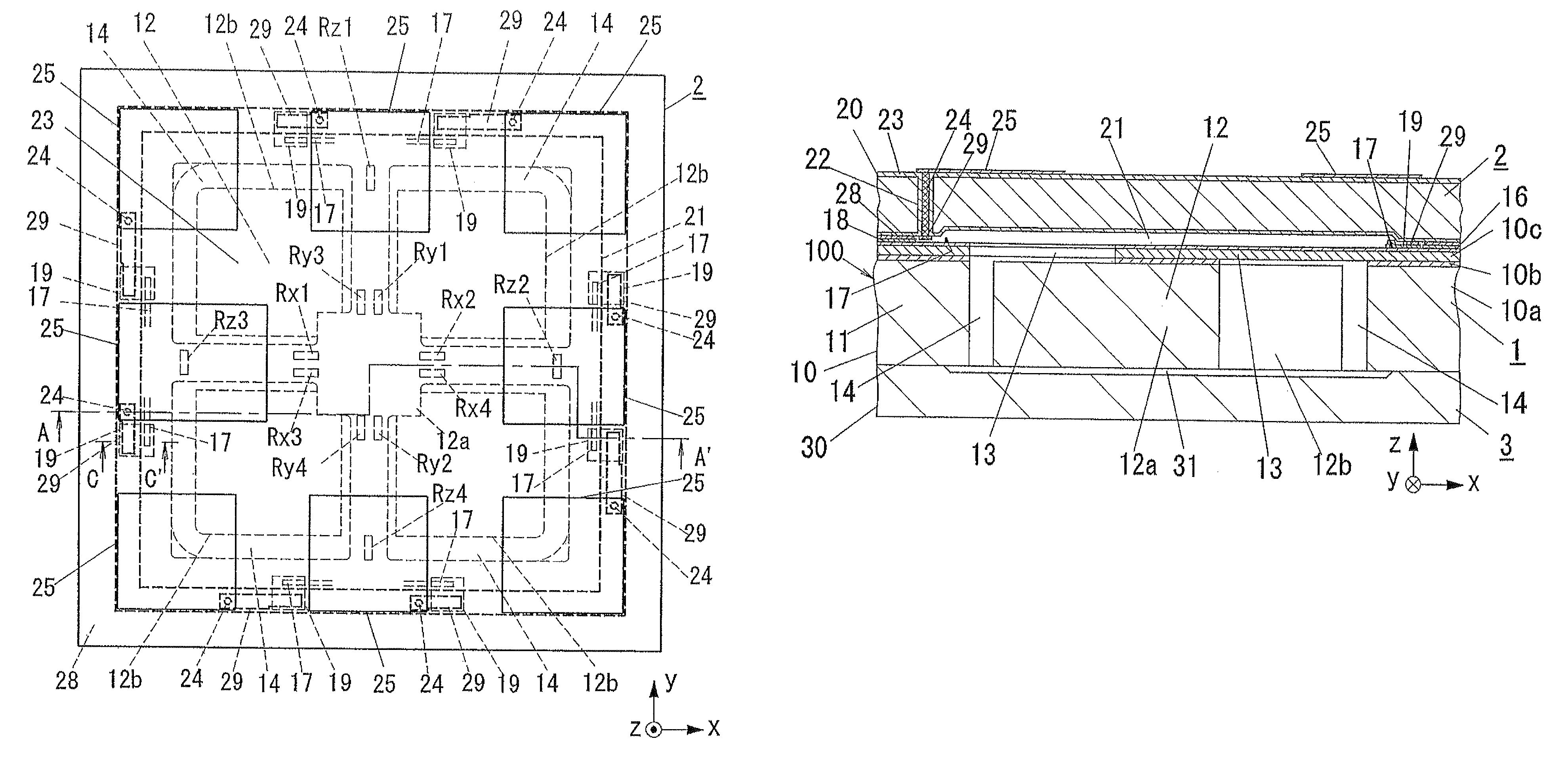
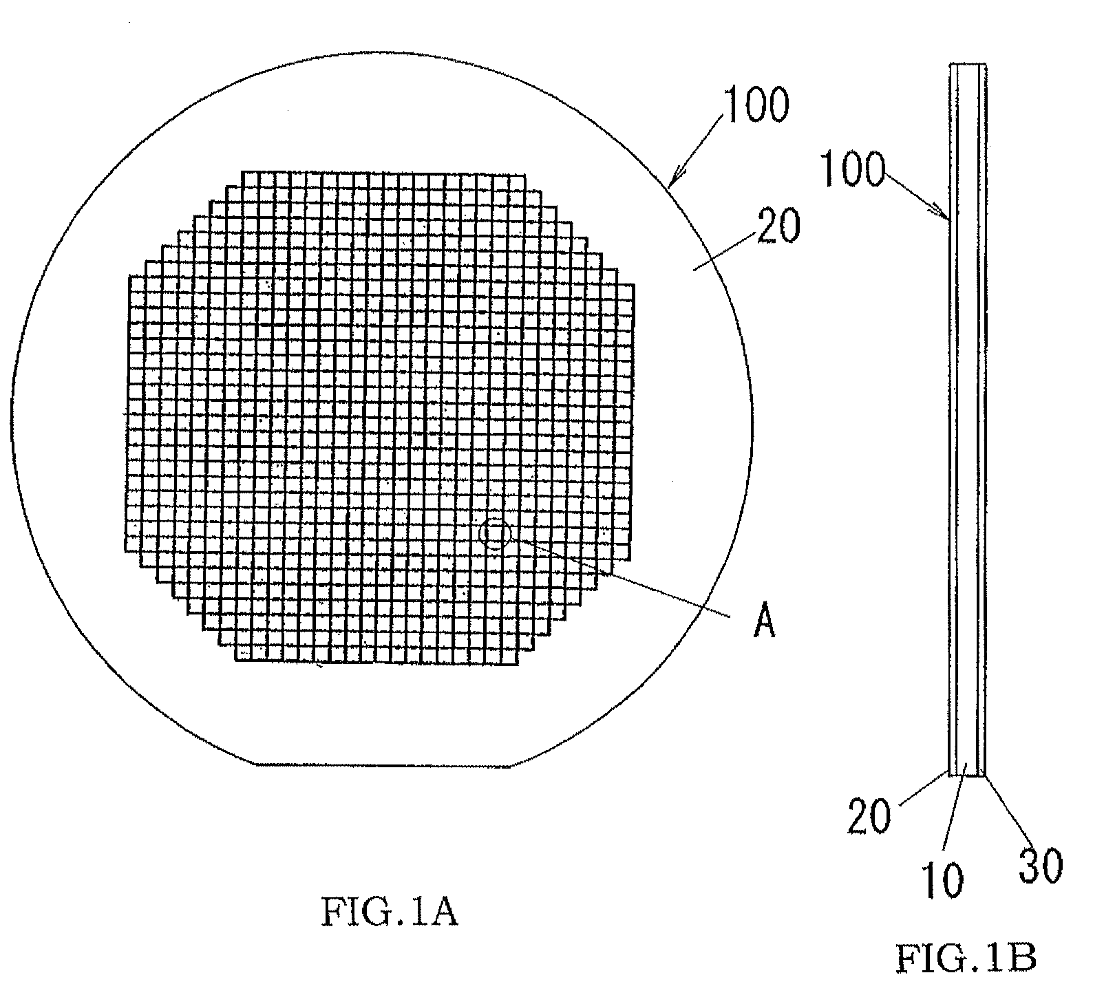
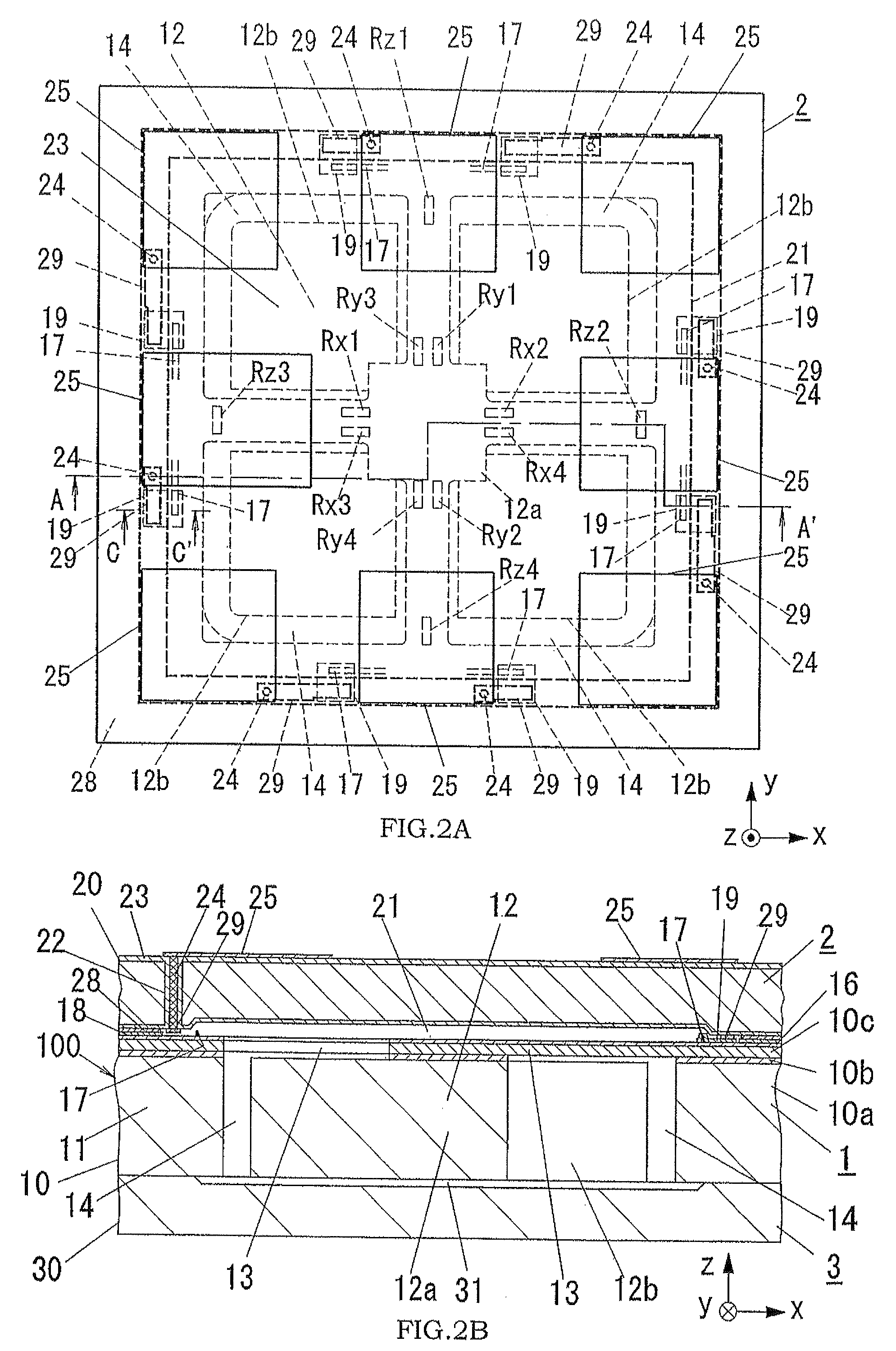
[0058]In the present embodiment, as shown in FIGS. 1A, 1B and FIGS. 2A and 2B, it is explained about a case where a sensor device is produced by fabricating a wafer level package structure 100 comprising a semiconductor wafer 10, in which a plurality of acceleration sensor units are integrally formed, a first package wafer 20 bonded to one of opposite surfaces of the semiconductor wafer 10, and a second package wafer 30 bonded to the other surface of the semiconductor wafer 10, and then dicing the wafer level package structure 100 into a size of the sensor device. Therefore, in the sensor device of the present embodiment, a portion corresponding to the semiconductor wafer 10 is defined as a sensor substrate 1. A portion corresponding to the first package wafer 20 is defined as a first package substrate 2. A portion corresponding to the second package wafer 30 is defined as a second package substrate 3.
[0059]The present embodiment of producing sensor devices from the wafer level pack...
second embodiment
[0098]As shown in FIGS. 14A to 14C, a wafer level package structure of the present embodiment is substantially the same as that of the first embodiment except that the sensor substrate 1 has an IC region E2 other than an acceleration sensor unit, and the IC region E2 comprises an integrated circuit (i.e., CMOS IC) using CMOS and operable in collaboration with the piezoresistive elements (Rx1 to Rx4, Ry1 to Ry4, Rz1 to Rz4) of gauge resistances (i.e., a sensing portion). The integrated circuit is formed by integrating a signal processing circuit configured to execute signal processing such as amplification, offset adjustment and temperature compensation to output signals of the bridge circuits (Bx, By, Bz) explained in the first embodiment, and an EEPROM for storing data used in the signal processing circuit. Therefore, in the following explanation, the same components as those in the first embodiment are denoted by the same reference numerals, and the duplicate explanation will be o...
third embodiment
[0119]In each of the above embodiments, the piezoresistance-type acceleration sensor was used as the sensor unit. The technical concept of the present invention is also available to the other sensor unit such as a capacitance type acceleration sensor or a gyro sensor. The present embodiment is characterized by forming a gyro sensor unit on a sensor substrate in place of the acceleration sensor unit. The other configurations of the present embodiment are substantially the same as those of the first embodiment. Therefore, a bonding portion between the sensor substrate 101 and each of the first and second package substrates (102, 103) can be formed according to the same manner as the first embodiment.
[0120]A wafer level package structure of the present embodiment has a structure comprising a semiconductor wafer with a plurality of gyro sensor units, a first package wafer bonded to one of opposite surfaces of the semiconductor wafer, and a second package wafer bonded to the other surfac...
PUM
 Abstract
Description
Claims
Application Information
 - R&D
- Intellectual Property
- Life Sciences
- Materials
- Tech Scout
- Unparalleled Data Quality
- Higher Quality Content
- 60% Fewer Hallucinations
Browse by: Latest US Patents, China's latest patents, Technical Efficacy Thesaurus, Application Domain, Technology Topic, Popular Technical Reports.
© 2025 PatSnap. All rights reserved.Legal|Privacy policy|Modern Slavery Act Transparency Statement|Sitemap|About US| Contact US: help@patsnap.com


