Self-pulsation nitride semiconductor laser device and method for fabricating the same

a technology of nitride and laser device, which is applied in the direction of semiconductor laser, laser details, electrical equipment, etc., can solve the problems of high reliability and high performance of gan-based semiconductor layer, and the gan-based semiconductor laser device with buried type structure has not been put to practical use, so as to achieve effective reduction of current guiding width of regrown layer buried in the opening, and stable characteristics

Inactive Publication Date: 2009-11-03
PANASONIC CORP
View PDF4 Cites 0 Cited by
  • Summary
  • Abstract
  • Description
  • Claims
  • Application Information

AI Technical Summary

Benefits of technology

[0018]The present inventors found that a hole generated through the UV irradiation has a property to move to the face of the group V element of a GaN-based semiconductor and hence the etching is not proceeded on the face of the group III element. The inventors thought that etching of the current blocking layer (the face thereof of the group III element) cannot be stably performed because of this phenomenon. When the current blocking layer was etched with the reverse face (the face of the group V element) of the GaN substrate protected from the etching solution, the etching could be performed stably.
[0019]Through application of this etching method, a GaN-based semiconductor laser device with a buried type structure could be stably obtained, and as a result, the characteristics of the semiconductor laser device could be evaluated with high reproducibility.
[0026]The cause of such a change to the n-type conductivity is not obvious, but the following seems to be one factor: When the p-type GaN guiding layer 3 is regrown, a portion thereof regrown from the side face of the opening 4 easily incorporates an n-type impurity or a defect functioning as a donor is easily caused.
[0030]When the width the n-type conductivity changed portion is increased and a substantial width of the guiding layer is reduced, a resistance component is increased in this portion, which can degrade the electric characteristics.
[0035]In this self-pulsation nitride semiconductor laser device, a current guiding width of the regrown layer buried in the opening can be reduced by changing the portion of the p-type regrown layer adjacent to the side face of the opening and having the given width into an n-type conductivity changed portion. This leads to an effect equivalent to that attained by effectively reducing the width of the opening of the current blocking layer. Therefore, when the opening is formed with a large width and the regrown layer is formed so as to cover the opening, the crystallinity of the regrown layer can be kept as well as the n-type conductivity changed portion is formed in a self-alignment manner to be adjacent to the side face of the opening, so that a current blocking structure in which the width of the opening is effectively reduced can be obtained. In other words, when the width of the n-type conductivity changed portion is controlled so that the effective current guiding width cannot exceed a width necessary for the self oscillation, a self-pulsation nitride semiconductor laser device having stable characteristics can be realized.
[0040]In the self-pulsation nitride semiconductor laser device and the method for fabricating the same according to the present invention, a portion of a p-type regrown layer adjacent to the side face of an opening of a current blocking layer is changed into an n-type conductivity changed portion having a given width. Therefore, a current guiding width of the regrown layer buried in the opening can be effectively reduced, so as to realize a self-pulsation nitride semiconductor laser device having stable characteristics.

Problems solved by technology

Although the processability of a current blocking layer and the crystallinity of a regrown layer can be improved by employing the technique described in Japanese Laid-Open Patent Publication No. 10-93199, a GaN-based semiconductor layer with high performance and high reliability has not been realized yet, and a GaN-based semiconductor laser device with the buried type structure has not been put to practical use.

Method used


Image

  • Self-pulsation nitride semiconductor laser device and method for fabricating the same
  • Self-pulsation nitride semiconductor laser device and method for fabricating the same
  • Self-pulsation nitride semiconductor laser device and method for fabricating the same

Examples


embodiment 1

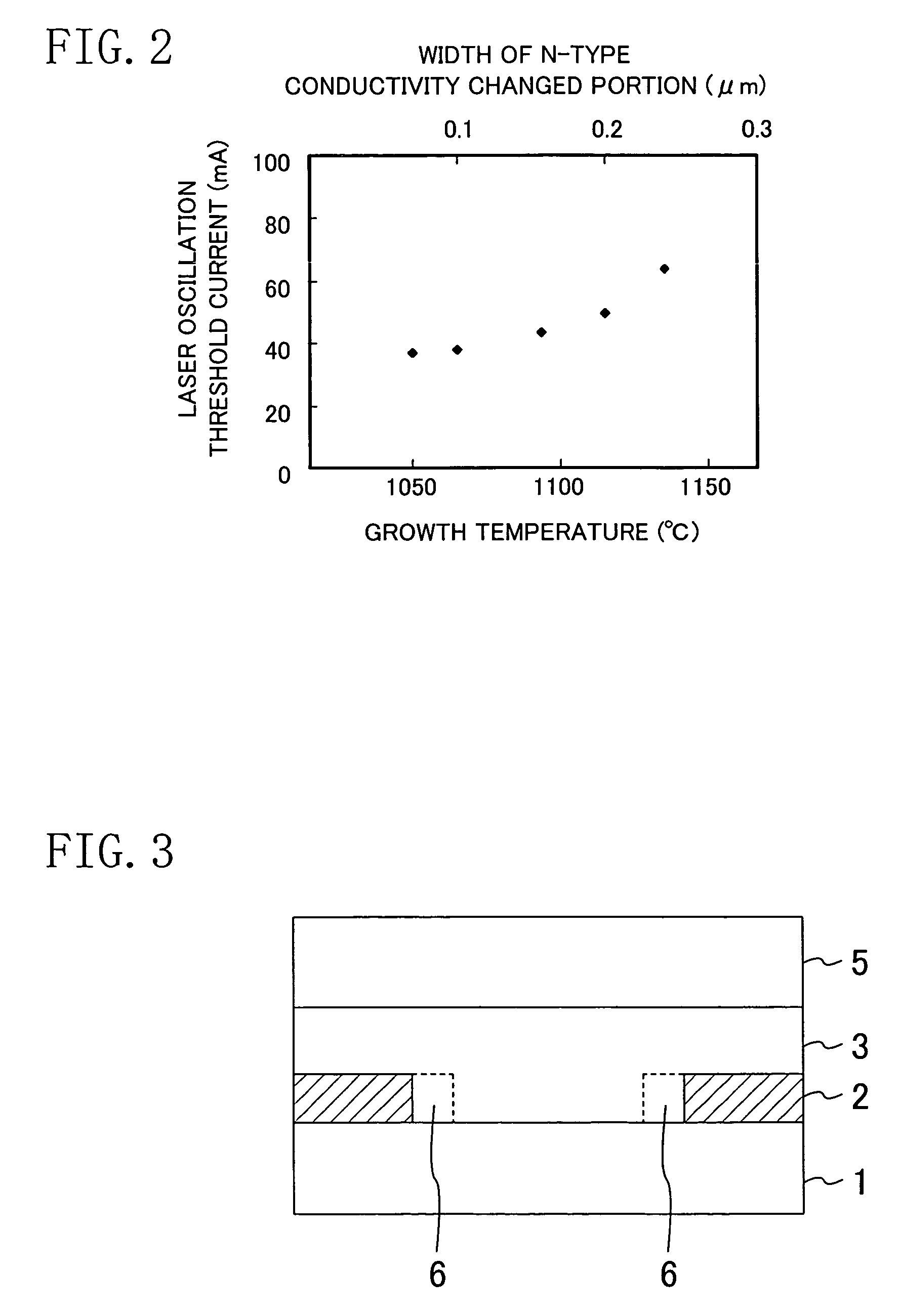
[0052]The present inventors have regarded a self-pulsation nitride semiconductor laser device as a device for positively utilizing an n-type conductivity changed portion formed in employing a buried type current blocking structure.

[0053]Although a violet semiconductor laser is suitable as a light source for optical disks such as next generation DVDs, external feedback noise occurring in a reproducing operation is a problem, and in one of known methods for overcoming the problem, a self oscillation phenomenon of a semiconductor laser is used.

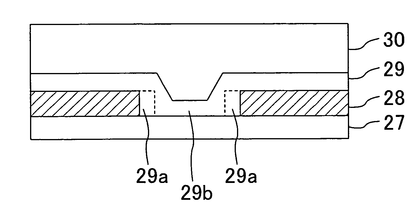
[0054]There are various conditions for causing the self oscillation of a semiconductor laser, and in a nitride semiconductor laser device having a buried type current blocking structure as shown in FIG. 3, it is necessary to set the width of the opening of the current blocking layer 2 to, for example, 1 μm or less.

[0055]When the opening is formed in the current blocking layer 2, the regrown layer 3 is formed so as to cover the opening. When the w...

embodiment 2

[0077]In Embodiment 1, the self-pulsation nitride semiconductor laser device is described as the device for positively utilizing an n-type conductivity changed portion. In this embodiment, application to another device will be described.

[0078]FIG. 8A through 8D are cross-sectional views for showing procedures in a method for fabricating a nitride semiconductor laser device according to Embodiment 2 of the invention.

[0079]First, as shown in FIG. 8A, an n-GaN layer 42, an n-Al0.06Ga0.94N cladding layer 43, an n-GaN guiding layer 44, an InGaN MQW active layer 45, a p-Al0.15Ga0.85N overflow suppressing layer 46, a p-GaN guiding layer 47 and a p-AlGaN cladding layer 48 are formed on a 2-inch GaN substrate 41 at a first stage of growth.

[0080]Next, as shown in FIG. 8B, a part of the p-AlGaN cladding layer 48 and the p-GaN guiding layer 47 is etched. In the case where it is difficult to completely remove the p-GaN guiding layer 47 without etching the p-Al0.15Ga0.85N overflow suppressing lay...


PUM


Abstract

In a buried type structure including an active layer sandwiched between an n-type cladding layer and a p-type cladding layer and a current blocking layer having an opening for confining a current flowing to the active layer, a regrown layer made of a nitride semiconductor doped with a p-type impurity is formed on the current blocking layer so as to cover the opening of the current blocking layer, and a portion of the regrown layer buried in the opening disposed to be adjacent to a side face of the opening and having a given width W is changed to have the n-type conductivity. Accordingly, the opening of the current blocking layer is effectively narrowed, so as to realize a self-pulsation nitride semiconductor laser device.

Description

CROSS-REFERENCE TO RELATED APPLICATIONS[0001]This application claims priority under 35 U.S.C. §119 on Patent Application No. 2006-053479 filed in Japan on Feb. 28, 2006, the entire contents of which are hereby incorporated by reference.BACKGROUND OF THE INVENTION[0002]The present invention relates to a nitride semiconductor laser device and a method for fabricating the same, and more particularly, it relates to a self-pulsation nitride semiconductor laser device having a buried type current blocking structure and a method for fabricating the same.[0003]Currently, a group III-V nitride-based compound semiconductor including group III elements of aluminum (Al), gallium (Ga) and indium (In) and a group V element of nitrogen (N), typified by gallium nitride (GaN) and represented by a general formula, InXGaYAl1-X-YN (wherein 0≦X≦1, 0≦Y≦1 and X+Y≦1), i.e., what is called a nitride semiconductor (hereinafter referred to as a GaN-based semiconductor), is regarded remarkable. With respect to...

Claims


Application Information

Patent Timeline
Patent Type & Authority Patents(United States)
IPC IPC(8): H01S5/00
CPCB82Y20/00H01S5/2231H01S5/34333H01S5/0658H01S5/2009H01S2304/00H01S5/221
Inventor TAMURA, SATOSHIIKEDO, NORIO
Owner PANASONIC CORP
Why Eureka
Try Eureka