
Semiconductor device having thin film transistor with particular drain electrode

a technology of semiconductor devices and drain electrodes, which is applied in semiconductor devices, optics, instruments, etc., can solve problems such as difficulty in obtaining large capacitance, and achieve the effect of high resistance to ions and high moisture resistan

Inactive Publication Date: 2009-01-27
SEMICON ENERGY LAB CO LTD
View PDF54 Cites 20 Cited by
  • Summary
  • Abstract
  • Description
  • Claims
  • Application Information

AI Technical Summary

Benefits of technology

The present invention provides a structure of an auxiliary capacitor that can provide a large capacitance while maintaining the area of the open portion (light-transmissive portion) of each pixel. This is achieved by using a conductive light-interruptive film over the active matrix side substrate, keeping it at a constant potential, and using it as one electrode of the auxiliary capacitor. The invention also includes various improvements related to the structure of the thin-film transistor, the conductive light-interruptive film, and the interlayer insulating film. The invention allows for efficient utilization of the available area of each pixel and provides a better barrier function for the display.

Problems solved by technology

However, it is difficult to obtain a large capacitance while maintaining the area of the open portion (light-transmissive portion) of each pixel.

Method used


Image

  • Semiconductor device having thin film transistor with particular drain electrode
  • Semiconductor device having thin film transistor with particular drain electrode
  • Semiconductor device having thin film transistor with particular drain electrode

Examples


embodiment 1

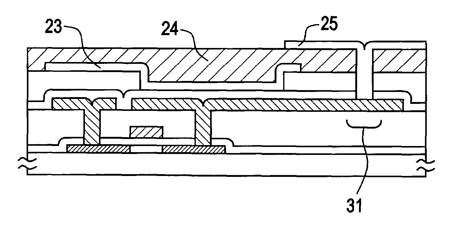
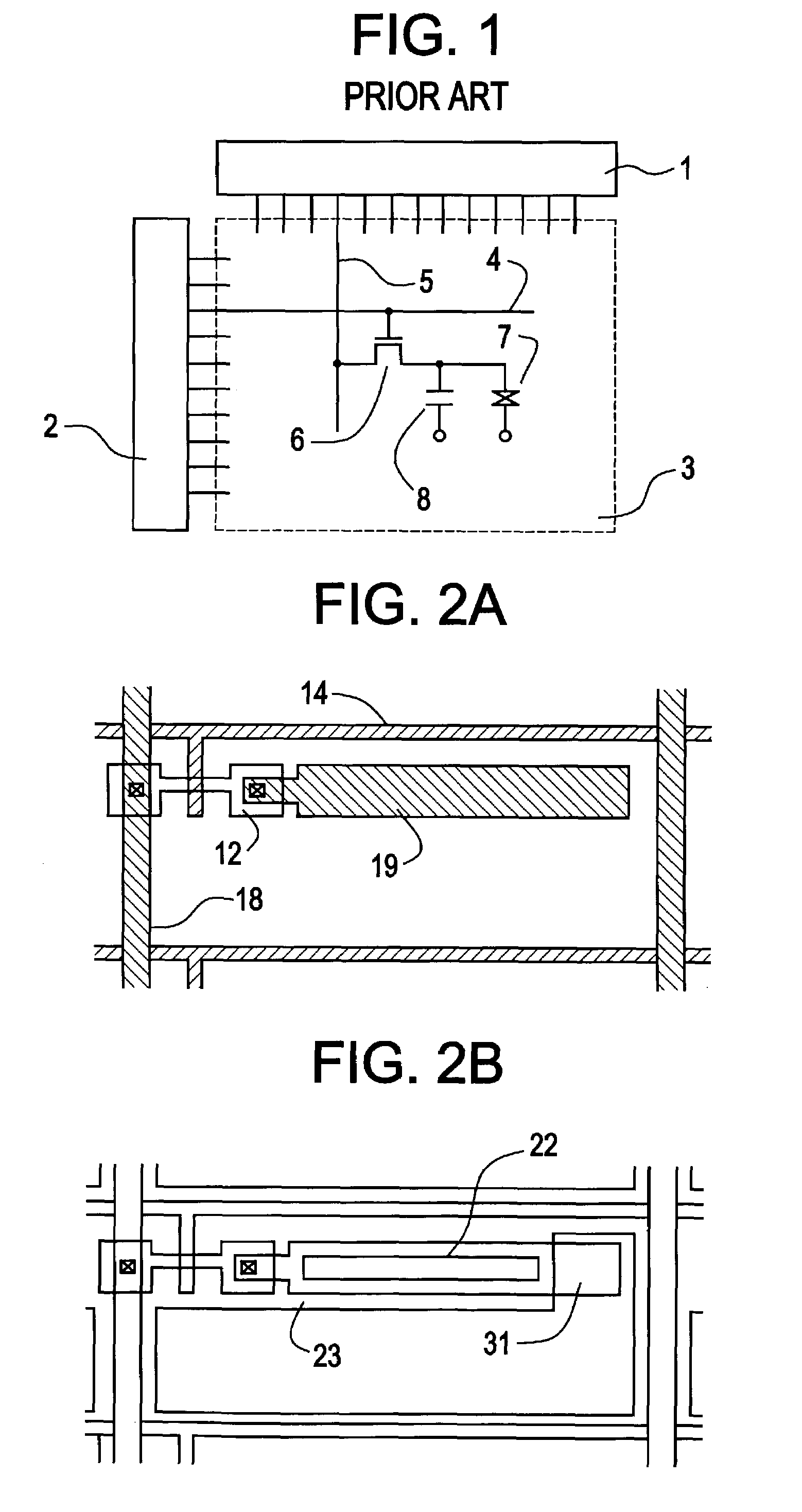
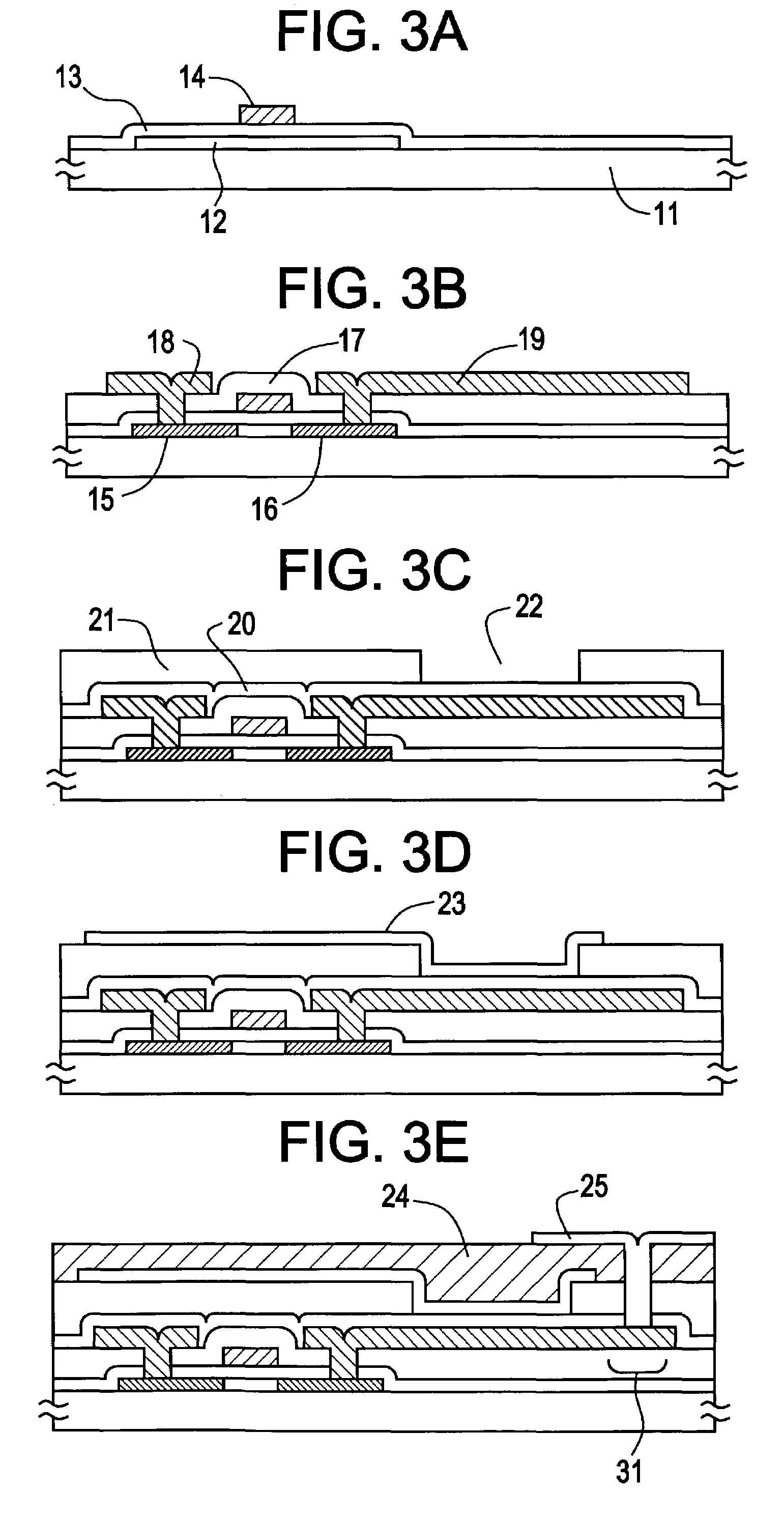
[0044]FIGS. 2A-2B and FIGS. 3A-3E are top views and sectional views, respectively, showing a manufacturing process according to this embodiment. The reference numerals used in FIGS. 2A-2B and FIGS. 3A-3E correspond to each other. Numerical values of the film thickness etc. used in the following embodiments are just examples and are not necessarily optimum ones, and a party to practice the invention is completely allowed to change those values when necessary.

[0045]First, a 500-Å-thick amorphous silicon film is formed over a glass substrate 11 by plasma CVD or low-pressure CVD. It is preferable to form a 3,000-Å-thick silicon oxide film as an underlayer film on the glass substrate 11 by sputtering or plasma CVD. The underlayer film may be omitted in a case of using a quartz glass substrate.

[0046]Then, an active layer 12 of a thin-film transistor is obtained by converting the amorphous silicon film into a crystalline silicon film by a known annealing technique such as heating or laser ...

embodiment 2

[0058]FIGS. 4A and 4B are top views showing a manufacturing processing according to this embodiment. The manufacturing process itself of this embodiment is almost the same as that of the first embodiment. The reference numerals commonly used in the first and second embodiments represent the same or equivalent parts. This embodiment is different from the first embodiment in circuit layout; that is, each pixel is formed efficiently (i.e., the effective aperture ratio is increased) by forming the auxiliary capacitor in a region where disclination is prone to occur.

[0059]FIG. 5 shows a pixel having the same circuit layout as the pixel according to the first embodiment. As shown in FIG. 5, disclination is prone to occur in a top-right region 30 of the pixel in a display device in which a pixel electrode contact 31 is provided at a top-right position of the pixel, rubbing is performed in the top-right to bottom-left direction (not bottom-left to top-right direction), and the source-line-i...

embodiment 3

[0063]FIGS. 6A and 6B are top views showing a manufacturing processing according to this embodiment. The manufacturing process itself of this embodiment is almost the same as that of the first embodiment. The reference numerals commonly used in the first and third embodiments represent the same or equivalent parts. Although the layout relating to the auxiliary capacitor in this embodiment is substantially the same as in the second embodiment, in this embodiment it is intended to utilize the available area of each pixel more efficiently by changing the layout relating to the active layer of the thin-film transistor.

[0064]In this embodiment, rubbing is performed in the bottom-left to top-right direction, in which case disclination is prone to occur in a bottom-left region. While in the second embodiment the auxiliary capacitor is provided in such a region where disclination is prone to occur, in this embodiment part of the active layer of the thin-film transistor of the next row is ad...


PUM

PropertyMeasurementUnit
thicknessaaaaaaaaaa
conductiveaaaaaaaaaa
areaaaaaaaaaaa

Abstract

A first insulating thin film having a large dielectric constant such as a silicon nitride film is formed so as to cover a source line and a metal wiring that is in the same layer as the source line. A second insulating film that is high in flatness is formed on the first insulating film. An opening is formed in the second insulating film by etching the second insulating film, to selectively expose the first insulating film. A conductive film to serve as a light-interruptive film is formed on the second insulating film and in the opening, whereby an auxiliary capacitor of the pixel is formed between the conductive film and the metal wiring with first the insulating film serving as a dielectric. The effective aperture ratio can be increased by forming the auxiliary capacitor in a selected region where the influences of alignment disorder of liquid crystal molecules, i.e., disclination, are large.

Description

BACKGROUND OF THE INVENTION[0001]1. Field of the Invention[0002]The present invention relates to the circuit configuration and layout of a pixel area of an active matrix display device in which thin-film transistors are used and source lines formed above gate lines. In particular, the invention relates to the structure of an auxiliary capacitor.[0003]2. Description of the Related Art[0004]In recent years, techniques of forming thin-film transistors (TFTs) on an inexpensive glass substrate have been made rapid progress. This is because of increased demand for the active matrix liquid crystal display device.[0005]In the active matrix liquid crystal display device, thin-film transistors are provided for respective ones of hundreds of thousands to millions of pixels that are arranged in matrix form and the charge entrance and exit to each pixel is controlled by the switching function of the thin-film transistor.[0006]A liquid crystal is interposed between each pixel electrode and an opp...

Claims


Application Information

Patent Timeline
Patent Type & Authority Patents(United States)
IPC IPC(8): G02F1/1343G02F1/136G02F1/1362G02F1/1368H01L21/336H01L21/77H01L21/84H01L27/12H01L27/13H01L29/786
CPCG02F1/136209G02F1/136213G02F1/136227H01L29/78645H01L27/1255H01L27/124
Inventor OHTANI, HISASHIOGATA, YASUSHI
Owner SEMICON ENERGY LAB CO LTD
Learn More