
Dual channel SiPM for optimal energy and fast timing

a dual-channel, fast timing technology, applied in the field of medical imaging systems, can solve the problems of fewer photons that can be collected, the size of the device needs to be compromised, and the device is too small to be used, so as to achieve high quantum efficiency, low noise, and high gain

Active Publication Date: 2008-10-21
SIEMENS MEDICAL SOLUTIONS USA INC
View PDF1 Cites 33 Cited by
  • Summary
  • Abstract
  • Description
  • Claims
  • Application Information

AI Technical Summary

Benefits of technology

[0010]SiPMs have the potential to become a replacement for photomultiplier tubes (PMTs) and avalanche photodiode (APDs) for use as photodetectors in positron emission topography (PET), Single photon emission computed tomography (SPECT), computed tomography (CT), and other radiation detectors. These devices are compact, have high gain, high quantum efficiency (about 20%-70%, which is better than that of traditional PMTs) and low noise. These devices have the potential to be used in time-of-flight PET applications due to their timing performance. They are also insensitive to magnetic fields, a quality which makes them ideal for use in an MR environment.

Problems solved by technology

However, as the size of the array increase, so does the capacitance and noise of the device.
However, the smaller the device is, the fewer photons that can be collected to be used for the 511 keV energy discrimination.
Thus, typically the size of the device needs to be compromised, resulting in a device that is as large as needed for adequate light collection and energy resolution.

Method used


Image

  • Dual channel SiPM for optimal energy and fast timing
  • Dual channel SiPM for optimal energy and fast timing
  • Dual channel SiPM for optimal energy and fast timing

Examples


example

[0030]Because APDs are insensitive to magnetic fields, they can be used in PET modules with PET and / or MR imaging. Two, APD-based, PET modules have been evaluated for use in combined PET / MR imaging. Each module comprises 4 independent, optically isolated detectors. Each detector comprises an 8×8 array of 2 mm×2 mm×20 mm LSO crystals read out by a 2×2 array of 5 nm×5 mm Hamamatsu S8664-55 APDs. The average crystal energy resolution and time resolution (against a plastic scintillator on a PMT) of the detectors was 17% and 1.8 ns, respectively. The modules were positioned in the tunnel of a 1.5 Tesla Siemens Symphony MR scanner. The presence of the PET modules decreased the MR signal-to-noise ratio by about 15% but no image interference was observed. The gradient and RF pulse sequences of the MR produced adverse effects on the PET event signals. These high frequency pulses did not affect the true PET events but did increase the dead time of the PET system. Simultaneous, artifact-free, ...


PUM


Abstract

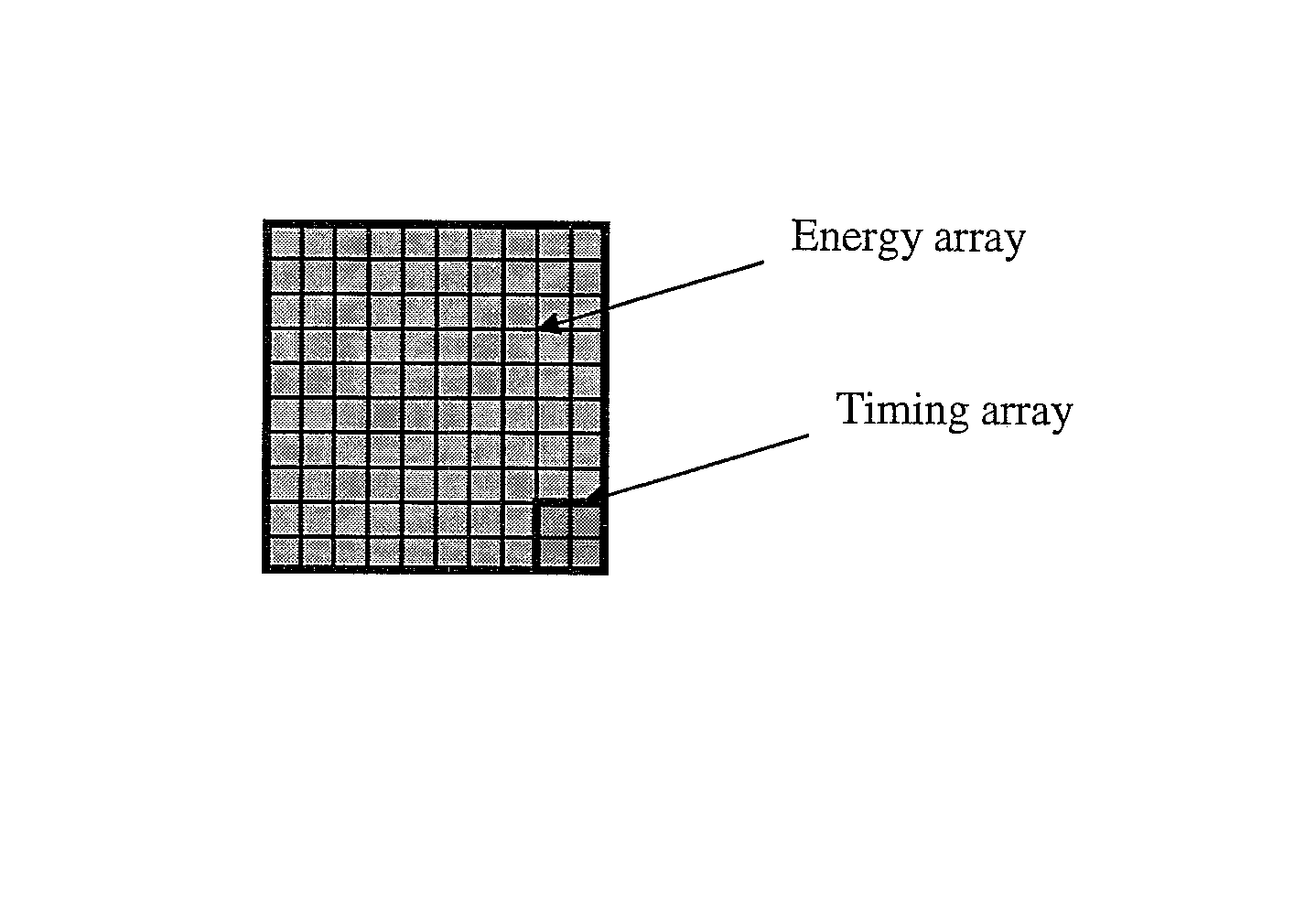
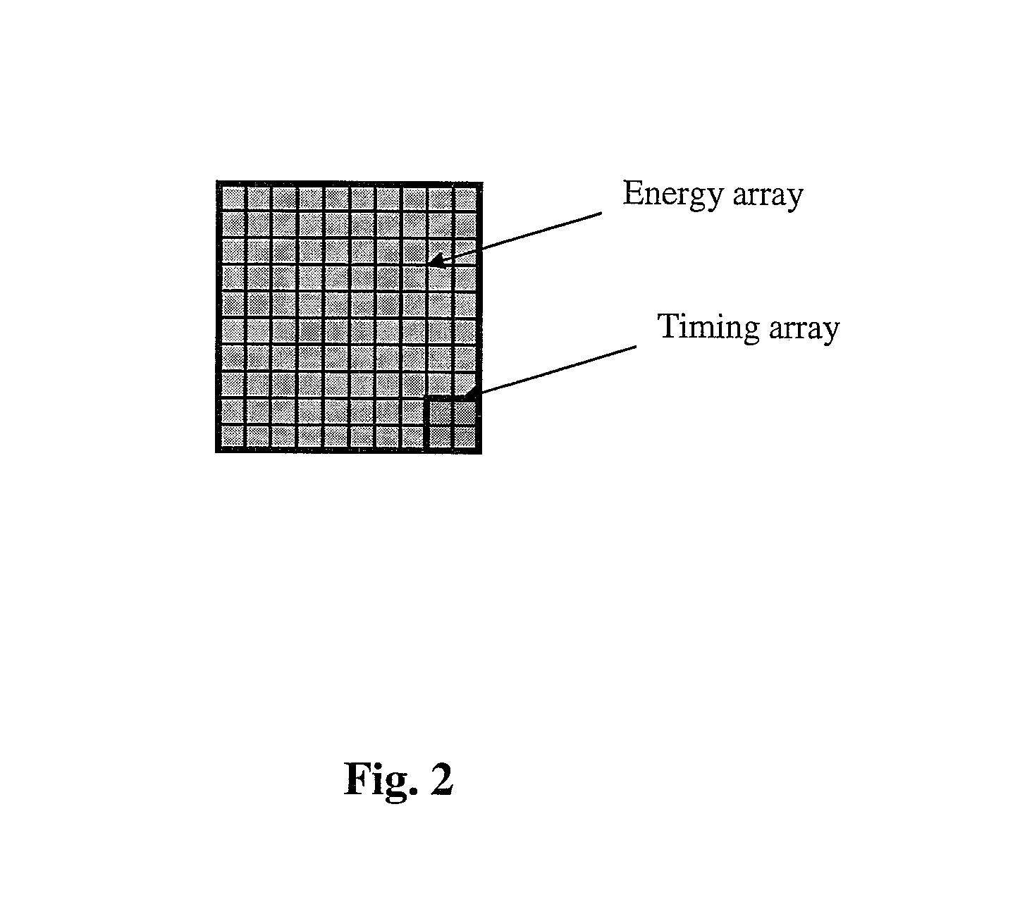
Dual channel silicon photomultipliers (SiPMs) can replace PMTs and APDs for use in PET and other radiation detectors. The devices are compact, have high gain, high QE and low noise. Due to their timing performance, these devices can be used in time-of-flight PET applications. By dividing the device into two separate channels, one for timing resolution and one for energy resolution, both can be optimized simultaneously.

Description

BACKGROUND[0001]1. Field of the Invention[0002]The present invention relates to medical imaging systems; more particularly, the present invention relates to silicon photomultipliers (SiPMs) in medical imaging systems.[0003]2. Description of Related Art[0004]SiPMs are semiconductor photon sensitive devices made up of an array of very small Geiger-mode avalanche photodiode (APD) cells on a silicon substrate. An example 10×10 microcell array is shown in FIG. 1. Each cell is connected to one another to form one larger device with one signal output. The entire device size can be as small as 1×1 mm or much larger.[0005]APD cells vary in dimension from 20 to 100 microns depending on the mask used, and can have a density of up to 1000 / sq. mm. Avalanche diodes can also be made from other semiconductors besides silicon, depending on the properties that are desirable. Silicon detects in the visible and near infrared range, with low multiplication noise (excess noise). Germanium (Ge) detects in...

Claims


Application Information

Patent Timeline
Patent Type & Authority Patents(United States)
IPC IPC(8): G01J5/20
CPCG01T1/2018G01T1/208G01T1/20184G01T1/20182
Inventor GRAZIOSO, RONALDZHANG, NAN
Owner SIEMENS MEDICAL SOLUTIONS USA INC
Learn More