
Wired circuit board

a wired circuit board and wire technology, applied in the direction of printed circuit non-printed electric components association, integrated arm assembly, instruments, etc., can solve the problem that the electrostatic breakdown of the mounted electronic components cannot be reliably prevented, and achieve the effect of improving the connection reliably of the wire circuit board and preventing the electrostatic breakdown of the mounted electronic components

Inactive Publication Date: 2008-10-07
NITTO DENKO CORP
View PDF6 Cites 4 Cited by
  • Summary
  • Abstract
  • Description
  • Claims
  • Application Information

AI Technical Summary

Benefits of technology

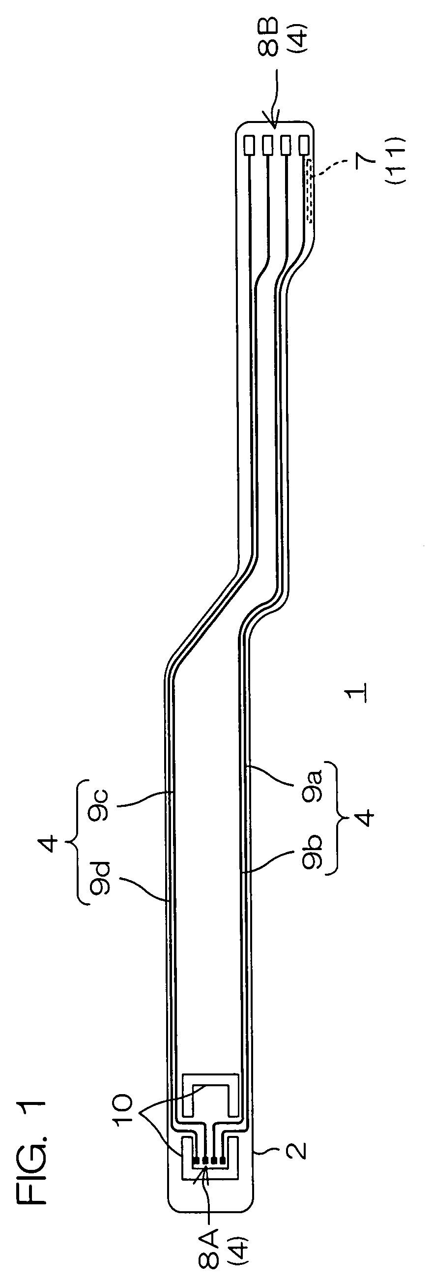
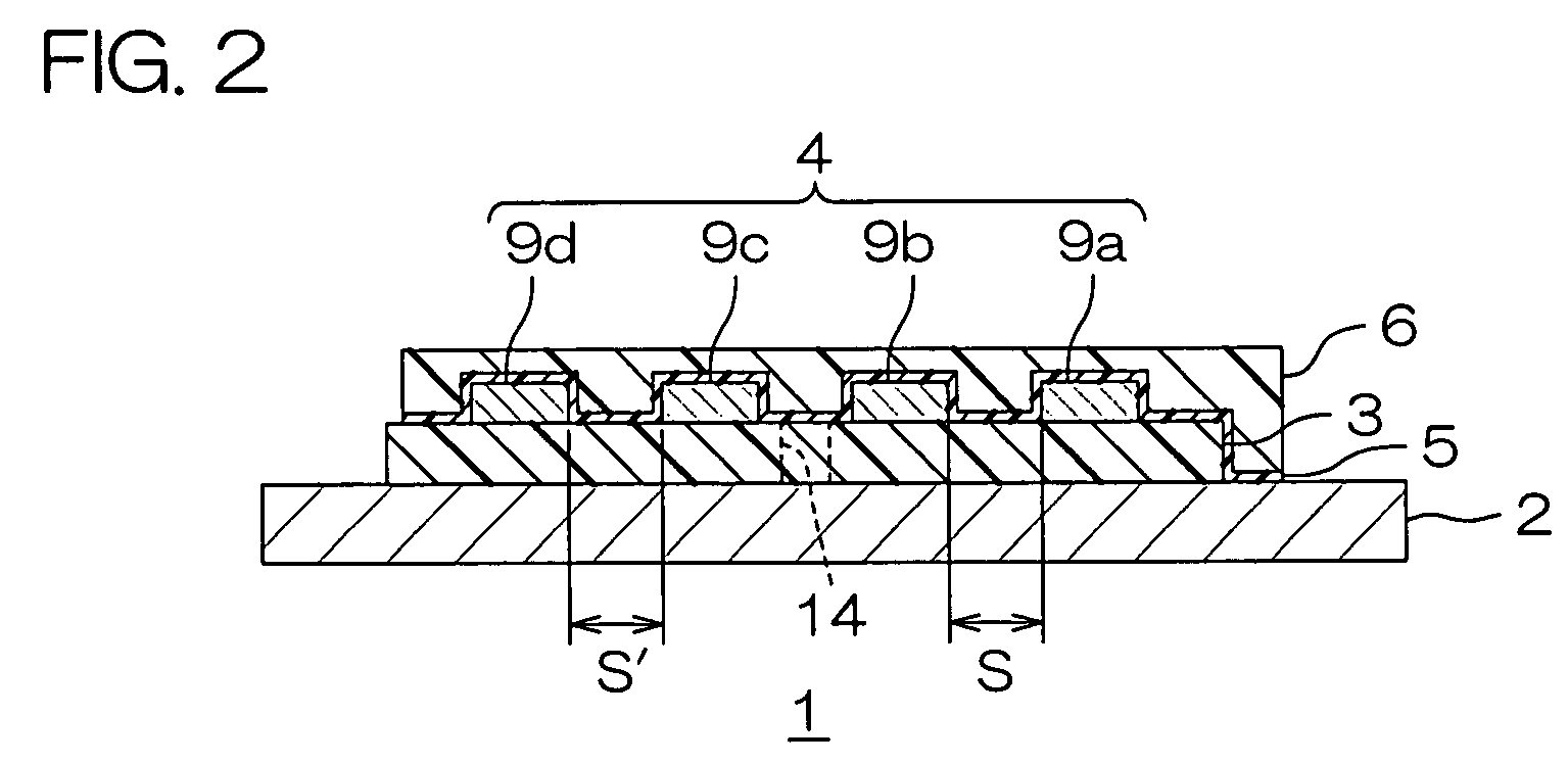
The present invention provides a wired circuit board that can efficiently remove electrostatic charging and prevent ion migration from a metal supporting board. The wired circuit board includes a metal supporting board, an insulating base layer, a conductive pattern, a semiconductive layer, and an insulating cover layer. The semiconductive layer is in contact with the metal supporting board on one side outside the region where the pair of wires are opposed, which prevents the formation of an electric field around the wires and ensures reliable prevention of ion migration. The insulating base layer has a base opening and a ground connection portion in contact with the metal supporting board, which further enhances the connection reliability of the wire circuit board.

Problems solved by technology

However, only the conductive polymer layer formed on the cover layer recited in Japanese Unexamined Patent Publication No. 2004-158480, is insufficient to remove the electrostatic charging, resulting in that the electrostatic breakdown of the mounted electronic component may not be prevented reliably.
As a result, a problem arises that the metal of the metal supporting board 32 migrates (ion migration) from the contact portion between the metal supporting board 29 and the semiconductive layer 35 into the insulating cover layer 36 due to the electric field E in such a loop-like shape.

Method used


Image

  • Wired circuit board
  • Wired circuit board
  • Wired circuit board

Examples


example 1

[0182]A metal supporting board made of a stainless steel foil having a thickness of 20 μm was prepared (see FIG. 3(a)).

[0183]Then, a varnish of a photosensitive polyamic acid resin was uniformly coated on a surface of the metal supporting board with a spin coater. Subsequently, the coated varnish was heated at 90° C. for 15 minutes to form a base coating. Thereafter, the base coating was exposed to light at 700 mJ / cm2 via a photomask, heated at 190° C. for 10 minutes, developed with an alkaline developer, and cured at 385° C. under a reduced pressure of 1.33 Pa, thereby forming an insulating base layer made of photosensitive polyimide on the metal supporting board to corresponded to the portion where a conductive pattern was formed and the peripheral end portion of the metal supporting board was exposed (see FIG. 3(b)). The thickness of the insulating base layer was 10 μm.

[0184]Then, a conductive pattern made of a copper foil and having a thickness of 10 μm was formed by an additive...

example 2

[0202]A metal supporting board made of a stainless steel foil having a thickness of 20 μm was prepared (see FIG. 5(a)).

[0203]Then, a varnish of a photosensitive polyamic acid resin was uniformly coated on a surface of the metal supporting board with a spin coater. Subsequently, the coated varnish was heated at 90° C. for 15 minutes to form a base coating. Thereafter, the base coating was exposed to light at 700 mJ / cm2 via a photomask, heated at 190° C. for 10 minutes, developed with an alkaline developer, and cured at 385° C. under a reduced pressure of 1.33 Pa, thereby forming an insulating base layer made of photosensitive polyimide on the metal supporting board to corresponded to the portion where a conductive pattern was formed and a base opening was formed therein (see FIG. 5(b)). The thickness of the insulating base layer was 10 μm. The base opening was in a rectangular shape when viewed in plan view having a width of 80 μm and a length of 100 μm.

[0204]Then, a conductive patte...


PUM


Abstract

A wired circuit board has a metal supporting board, an insulating base layer formed on the metal supporting board, a conductive pattern formed on the insulating base layer and including at least one pair of wires arranged in mutually spaced-apart and opposed relation having different potentials, a semiconductive layer formed on the insulating base layer to cover the conductive pattern and electrically connected to the metal supporting board on one side outside a region where the pair of wires are opposed, and an insulating cover layer formed on the semiconductive layer.

Description

CROSS-REFERENCE TO RELATED APPLICATION[0001]The present application claims priority from Japanese Patent Application No. 2006-127624 filed on May 1, 2006, the content of which is hereby incorporated by reference into this application.BACKGROUND OF THE INVENTION[0002]1. Field of the Invention[0003]The present invention relates to a wired circuit board and, more particularly, to a wired circuit board such as a suspension board with circuit on which an electronic component is mounted.[0004]2. Description of Related Art[0005]A wired circuit board such as a suspension board with circuit comprises, e.g., a metal supporting board made of a stainless steel foil or the like, an insulating base layer made of a polyimide resin or the like and formed on the metal supporting board, a conductive pattern made of a copper foil or the like and formed on the insulating base layer, and an insulating cover layer made of a polyimide resin or the like and formed on the insulating base layer to cover the ...

Claims


Application Information

Patent Timeline
Patent Type & Authority Patents(United States)
IPC IPC(8): H05K7/00
CPCG11B5/486H05K1/0259H05K1/056H05K1/167H05K3/28H05K2201/09554G11B5/484
Inventor ISHII, JUNOOYABU, YASUNARI
Owner NITTO DENKO CORP
Learn More