Fabrication of metallic microstructures via exposure of photosensitive composition
a technology of photosensitive composition and fabrication method, which is applied in the direction of liquid/solution decomposition chemical coating, photomechanical apparatus, instruments, etc., can solve the problems of not being available to every laboratory, requiring limited availability, and unable to meet the requirements of the laboratory, so as to achieve the effect of short production tim
- Summary
- Abstract
- Description
- Claims
- Application Information
AI Technical Summary
Benefits of technology
Problems solved by technology
Method used
Image
Examples
example 1
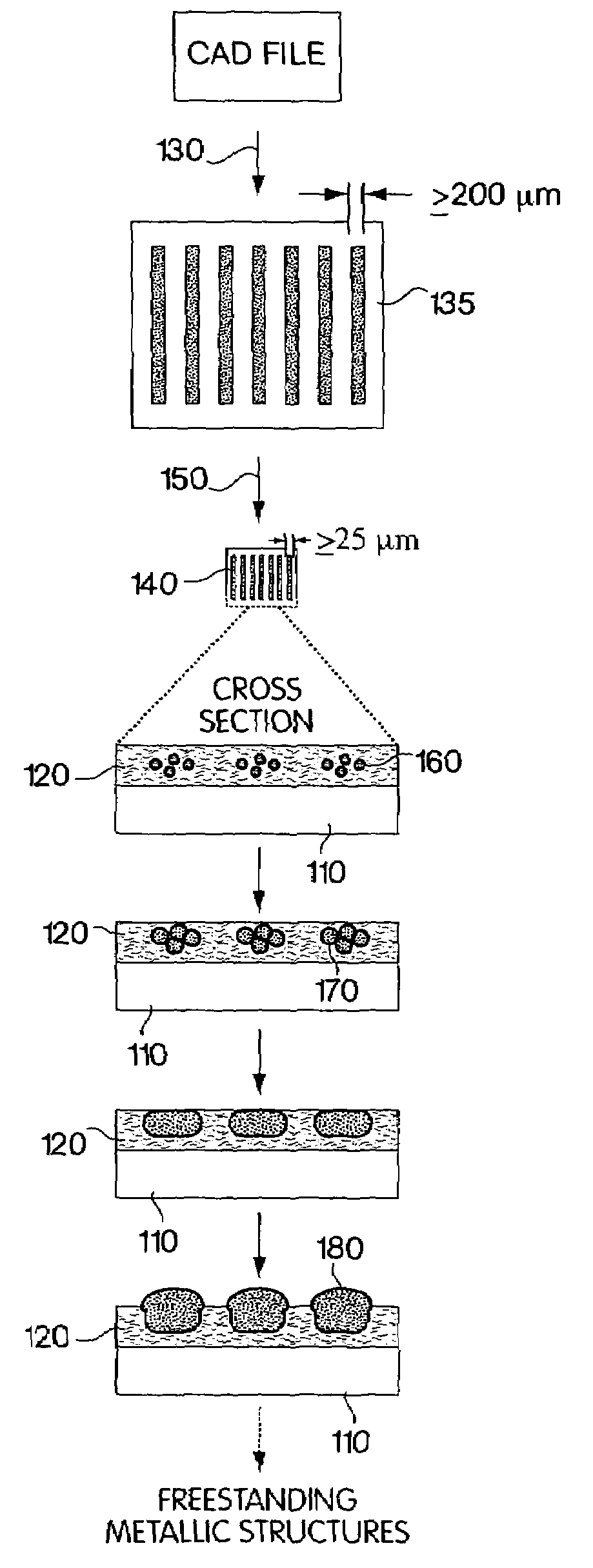
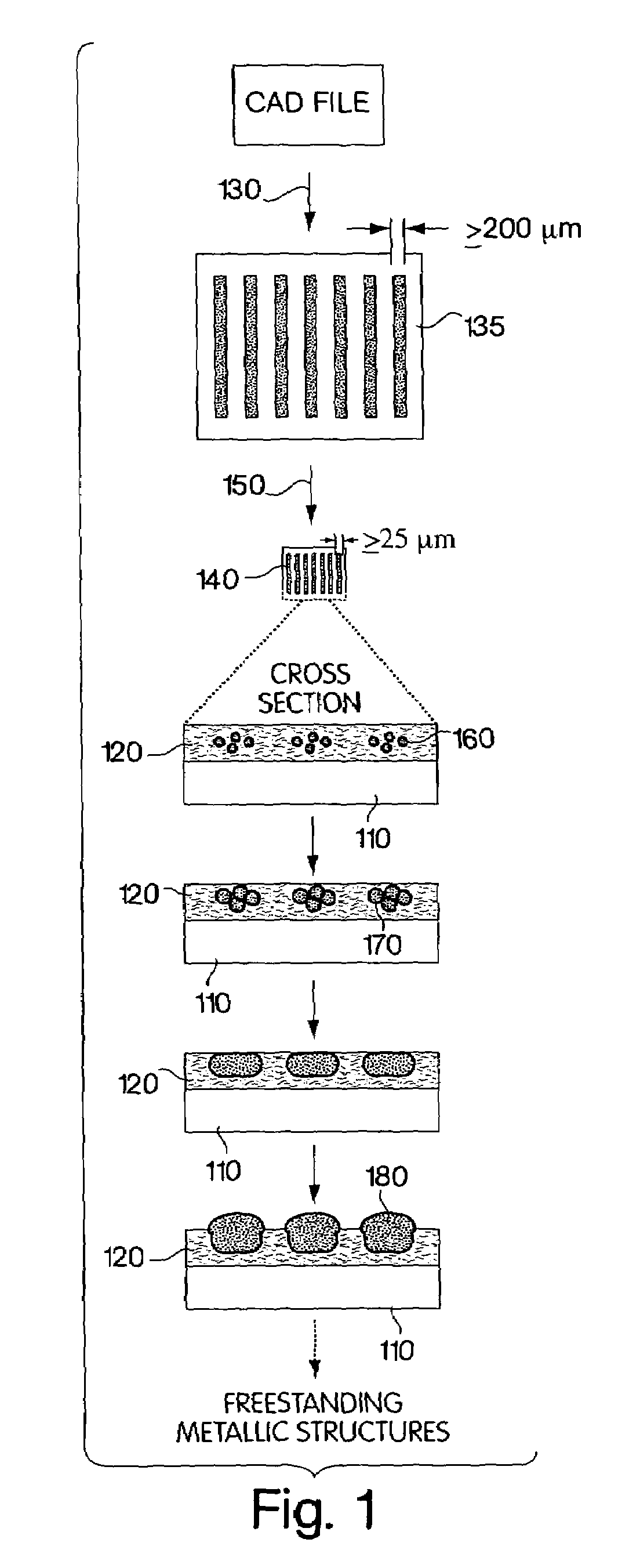
[0039]FIG. 1 illustrates an exemplary procedure used to fabricate metallic microstructures using silver halide-based photographic film. One element in this film is a substrate 110, a polyester backing (typically ˜100 μm thick) covered with a gelatin layer 120 (typically ˜2 μm thick) that contains silver halide. (Keller, K. Science and Technology of Photography; VCH: Weinheim, German, 1993.) A CAD file was first printed (130) on paper 135 with a 600 dpi office printer. A commercial slide maker was then used to reproduce (150) the black and white image on the silver halide-based photographic film 140. The initially developed film leaves the silver particles 160 isolated, with no electrically continuous path connecting adjacent portions in the pattern. Electroless deposition of additional silver, catalyzed by these silver grains, increased the grain size so that the grains come into contact 170. (Bjelkhagen, H. I. Silver-Halide Recording Materials for Holography and Their Processing; S...
example 2
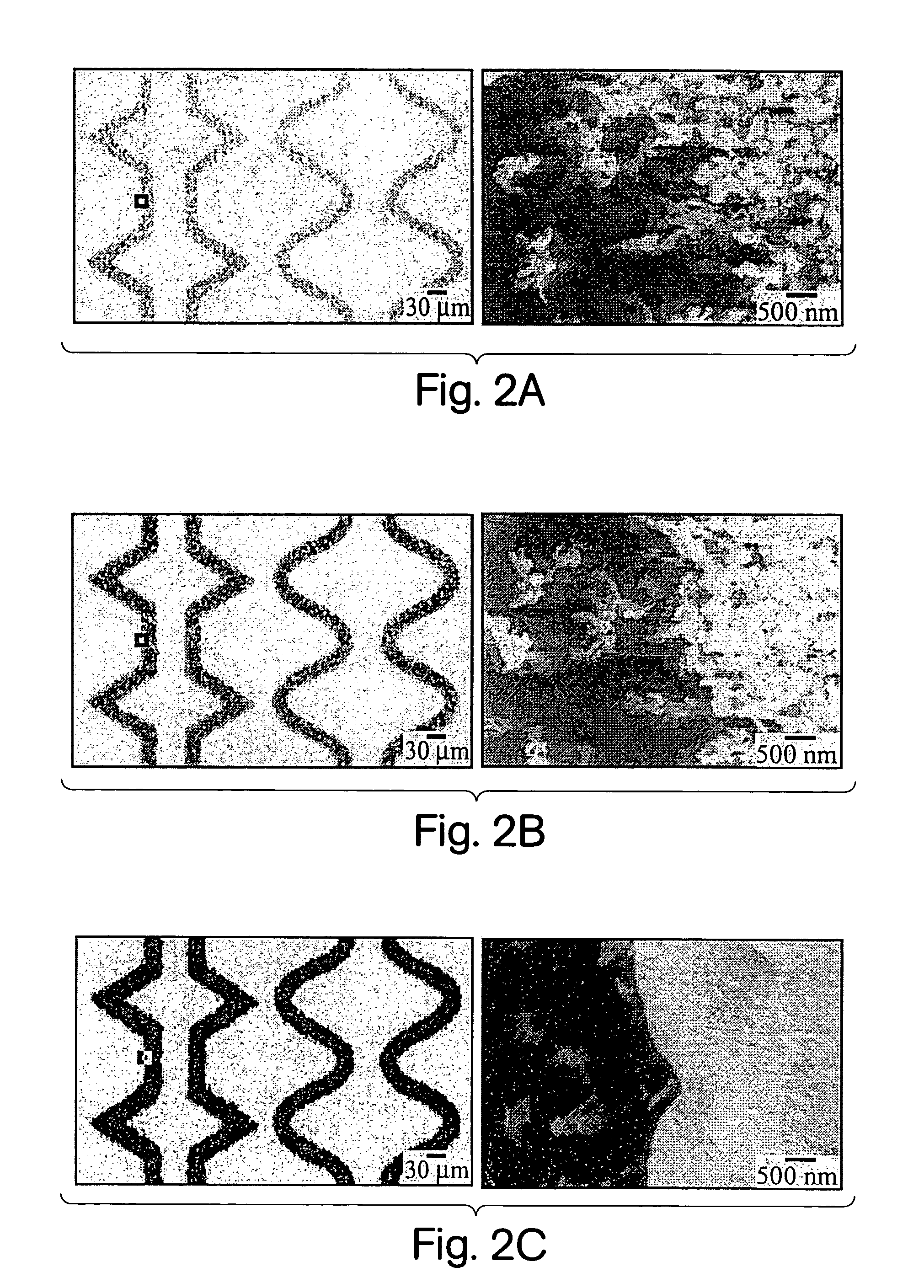
[0040]FIG. 2 shows optical micrographs of metallic lines (˜30 μm wide) generated by each of the steps in the fabrication process described above in Example 1. After development of the photographic image and before electroless deposition (FIG. 2a), the primary pattern of silver halide grains had a line width of ˜25 ∞m and an edge roughness of ˜2 μm. After electroless plating (FIG. 2b), the line width increased to ˜26 μm and the edge roughness remained approximately the same. After electroplating (FIG. 2c), a line width of ˜30 μm and an edge roughness of ˜3 μm were observed. The limited optics of the slide maker resulted in distorted, incomplete reproduction of patterns with smaller features. The edge roughness of patterns printed on the paper also contributed to the resolution of the final pattern, but it was not the major factor. The smallest feature sizes of metallic structures obtained using a master pattern printed with a 3387 dpi high-resolution image-setter were still ˜30 μm, w...
example 3
[0041]FIG. 3a shows a gold serpentine wire (˜50 μm wide and ˜2.5 μm thick; total length of ˜648 mm) fabricated to test the electrical continuity of metallic structures made using this procedure as described in Example 1. A uniform resistivity of ˜7×10⁻⁸ Ωm (FIG. 3b) was measured over the full length of the wire, which is ˜3.5 times higher than the value reported for pure bulk gold (˜2×10⁻⁸ Ωm). (Lide, D. R. CRC Handbook of Chemistry and Physics; CRC Press: New York, 1999.) A residual gelatin network, or a network of grain boundaries still present inside the wires after electroplating, are possible explanations for this difference.
PUM
| Property | Measurement | Unit |
|---|---|---|
| width | aaaaa | aaaaa |
| width | aaaaa | aaaaa |
| width | aaaaa | aaaaa |
Abstract
Description
Claims
Application Information
 - R&D
- Intellectual Property
- Life Sciences
- Materials
- Tech Scout
- Unparalleled Data Quality
- Higher Quality Content
- 60% Fewer Hallucinations
Browse by: Latest US Patents, China's latest patents, Technical Efficacy Thesaurus, Application Domain, Technology Topic, Popular Technical Reports.
© 2025 PatSnap. All rights reserved.Legal|Privacy policy|Modern Slavery Act Transparency Statement|Sitemap|About US| Contact US: help@patsnap.com


