
Low metal porous silica dielectric for integral circuit applications

a technology of low metal porous silica and integrated circuit, which is applied in the direction of resistive material coating, metallic material coating process, pretreatment surface, etc., can solve the problems of interconnect rc delay, power consumption and signal cross-talk becoming increasingly difficult to solve, and requiring heating for both aging or condensing process

Active Publication Date: 2008-06-03
HONEYWELL INT INC
View PDF16 Cites 20 Cited by
  • Summary
  • Abstract
  • Description
  • Claims
  • Application Information

AI Technical Summary

Benefits of technology

The invention provides a method for making a nanoporous silica dielectric film by coating a substrate with a composition containing a silicon-containing pre-polymer, a porogen, and a metal-ion-free catalyst. The composition is then crosslinked to form a gelled film, which is heated to remove the porogen. The invention also provides a composition containing silicon-containing pre-polymer, a porogen, and a catalyst selected from onium compounds and nucleophiles. The invention also describes a method for lowering the temperature at which a porous silica film forms by adding onium ions or nucleophiles to a silicon-containing pre-polymer and porogen.

Problems solved by technology

As feature sizes in integrated circuits are reduced to below 0.15 μm and below, problems with interconnect RC delay, power consumption and signal cross-talk have become increasingly difficult to resolve.
This process, like many of the previously employed methods of forming nanoporous films on semiconductors, has the disadvantage of requiring heating for both the aging or condensing process, and for the removal of a polymer to form the nanoporous film.
Furthermore, there is a disadvantage that organic polysilica, contained in a precursor solution, tends to increase in molecular weight after the solution is prepared; consequently, the viscosity of such precursor solutions increases during storage, and the thickness of films made from stored solutions will increase as the age of the solution increases.
The instability of organic polysilica thus requires short shelf life, cold storage, and fine tuning of the coating parameters to achieve consistent film properties in a microelectronics / integrated circuit manufacturing process.

Method used


Image

  • Low metal porous silica dielectric for integral circuit applications
  • Low metal porous silica dielectric for integral circuit applications

Examples


example 1

[0096]This example shows the production of a nanoporous silica with a porogen having a high concentration of sodium. A precursor was prepared by combining, in a 100 ml round bottom flask (containing a magnetic stirring bar), 10 g tetraacetoxysilane, 10 g methyltriacetoxysilane, and 17 g propylene glycol methyl ethyl acetate (PGMEA). These ingredients were combined within an N2-environment (N2 glove bag). The flask was also connected to an N2 environment to prevent environmental moisture from entering the solution (standard temperature and pressure).

[0097]The reaction mixture was heated to 80° C. before 1.5 g of water was added to the flask. After the water addition is complete, the reaction mixture was allowed to cool to ambient before 4.26 g of polyethylene glycol monomethylether (“PEO”; MW550 amu) (with >300 ppb Na) was added as a porogen, and stirring continued for another 2 hrs. Thereafter, the resulting solution was filtered through a 0.2 micron filter to provide the precursor ...

example 3

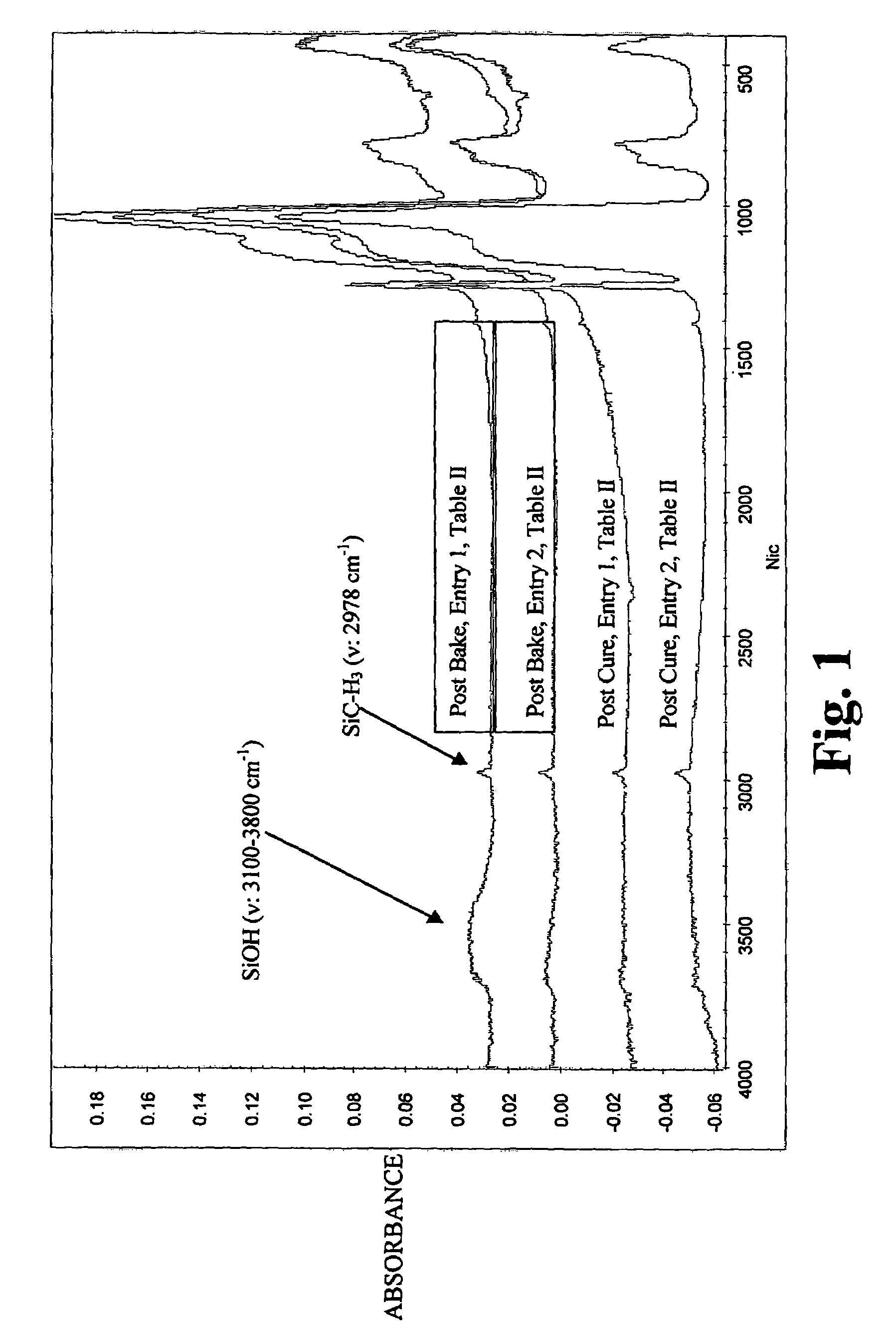
[0100]Example 2 is repeated except this example adds sodium cation (sodium hydroxide (see entry 3), or sodium sulfate (see entry 4) to restore the low k. Sodium hydroxide (NaOH, 23 ppm) or sodium sulfate (Na2SO4, 40 ppm) was were added to the ion-exchanged PEO and the precursor masterbatch. Films are deposited onto a wafer by spin coating at 2400 rpm or 3500 rpm. After spin coating, the film is heated in three hot plates at temperatures of 80° C., 175° C. and 300° C., one minute each. After bake, the film is cured under flowing nitrogen at 425° C. for one hour. The results of k and R.I. of the post-cure films are listed in the following table.

example 4

[0101]Example 2 is repeated except this example adds tetraorganoammonium (TMAA) (entries 5, 6, and 7), TMAH (entry 8), or TBAA (entry 9)) ion to restore the low k. Various amounts of TMAA were added to the ion-exchanged PEO and the precursor masterbatch. In some cases, small amount of methyltriacetoxysilane (MTAS, 1%, see entry 6) were added to the solution to serve as an in-situ surface modifier to make the surface less hydrophilic. Films were deposited onto a wafer by spin coating at 2400 rpm or 3500 rpm. After spin coating, the film was heated in three hot plates at temperatures of 80° C., 175° C. and 300° C., one minute each. After bake, the film was cured under flowing nitrogen at 425° C. for one hour. For entries 5 and 6, the average pore size diameter was 2.5 nm. The results of k and R.I. of the post-cure films are listed in the following table. It is shown that the k value is below 2.5 when the concentration of the ammonium ion is greater than about 65×10−9 mole / gm of soluti...


PUM

PropertyMeasurementUnit
dielectric constantaaaaaaaaaa
pore diameteraaaaaaaaaa
decomposition temperatureaaaaaaaaaa

Abstract

The invention relates to the production of nanoporous silica dielectric films and to semiconductor devices and integrated circuits comprising these improved films. The nanoporous films of the invention are prepared using silicon containing pre-polymers and are prepared by a process that allows crosslinking at lowered gel temperatures by means of a metal-ion-free onium or nucleophile catalyst.

Description

BACKGROUND OF THE INVENTION[0001]1. Field of the Invention[0002]The present invention relates to the production of nanoporous silica dielectric films and to semiconductor devices and integrated circuits comprising these improved films. The nanoporous films of the invention are prepared using silicon containing pre-polymers and are prepared by a process that allows crosslinking at lowered gel temperatures by means of a metal-ion-free onium or nucleophile catalyst.[0003]2. Description of the Related Art[0004]As feature sizes in integrated circuits are reduced to below 0.15 μm and below, problems with interconnect RC delay, power consumption and signal cross-talk have become increasingly difficult to resolve. It is believed that the integration of low dielectric constant materials for interlevel dielectric (ILD) and intermetal dielectric (IMD) applications will help to solve these problems. While there have been previous efforts to apply low dielectric constant materials to integrated ...

Claims


Application Information

Patent Timeline
Patent Type & Authority Patents(United States)
IPC IPC(8): B05D3/02H01L21/768C08J9/26C09D183/02C09D183/04H01L21/316
CPCC08J9/26C09D183/02C09D183/04H01L21/02126H01L21/02203H01L21/02216H01L21/02282H01L21/31695C08J2201/046C08J2383/04Y10T428/249953
Inventor LEUNG, ROGER Y.DENG, ERICXIE, SONGYUANLU, VICTOR Y.
Owner HONEYWELL INT INC
Learn More