Slurry for CMP and CMP method
a technology of slurry and cmp, applied in the field of slurry, can solve the problems of difficult to obtain stable polishing characteristics, difficult to obtain high selectivity ratio, and reduced metal film polishing rate, etc., to achieve suppression of dishing, stable polishing characteristics, and high selectivity
- Summary
- Abstract
- Description
- Claims
- Application Information
AI Technical Summary
Benefits of technology
Problems solved by technology
Method used
Image
Examples
first embodiment
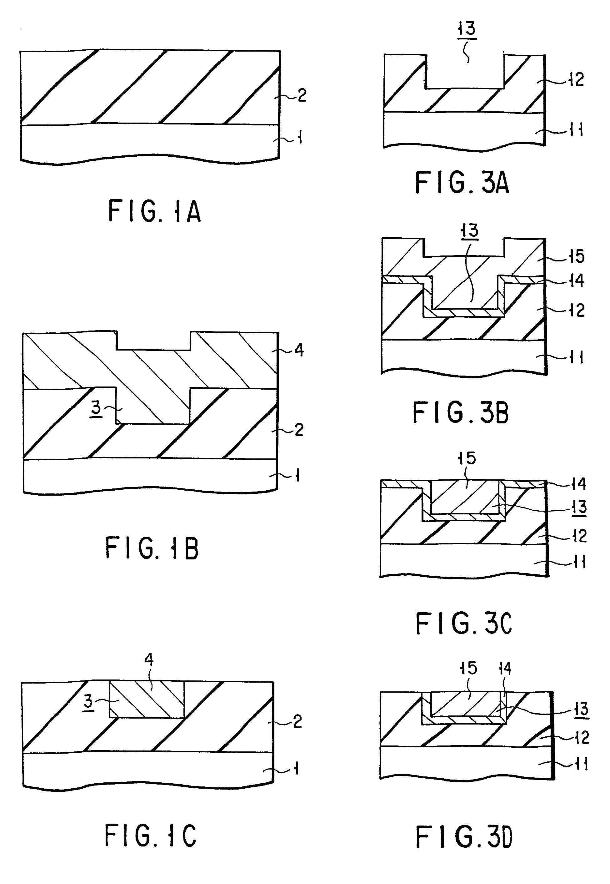
[0027]FIGS. 1A to 1C are cross-sectional views illustrating steps of a process of forming Al Damascene wiring according to a first embodiment of the present invention.
[0028]To start with, as shown in FIG. 1A, an SiO2 film 2 which serves as an interlayer insulating film is deposited on a silicon substrate 1 on which devices (not shown) are fabricated.
[0029]A wiring trench 3 is formed in a surface portion of the SiO2 film 2, as shown in FIG. 1B. Then, an Al film 4 for filling the wiring trench 3 is deposited on an entire surface of the resultant structure to a thickness of 600 nm.
[0030]At last, as shown in FIG. 1C, an excess portion of the Al film 4 outside the wiring trench 3 is removed by CMP using a slurry containing, as polishing abrasives, mixture (mixed-crystal) abrasives of silica and alumina and having a pH of 7. Thus, Al Damascene wiring 4 is completely formed.
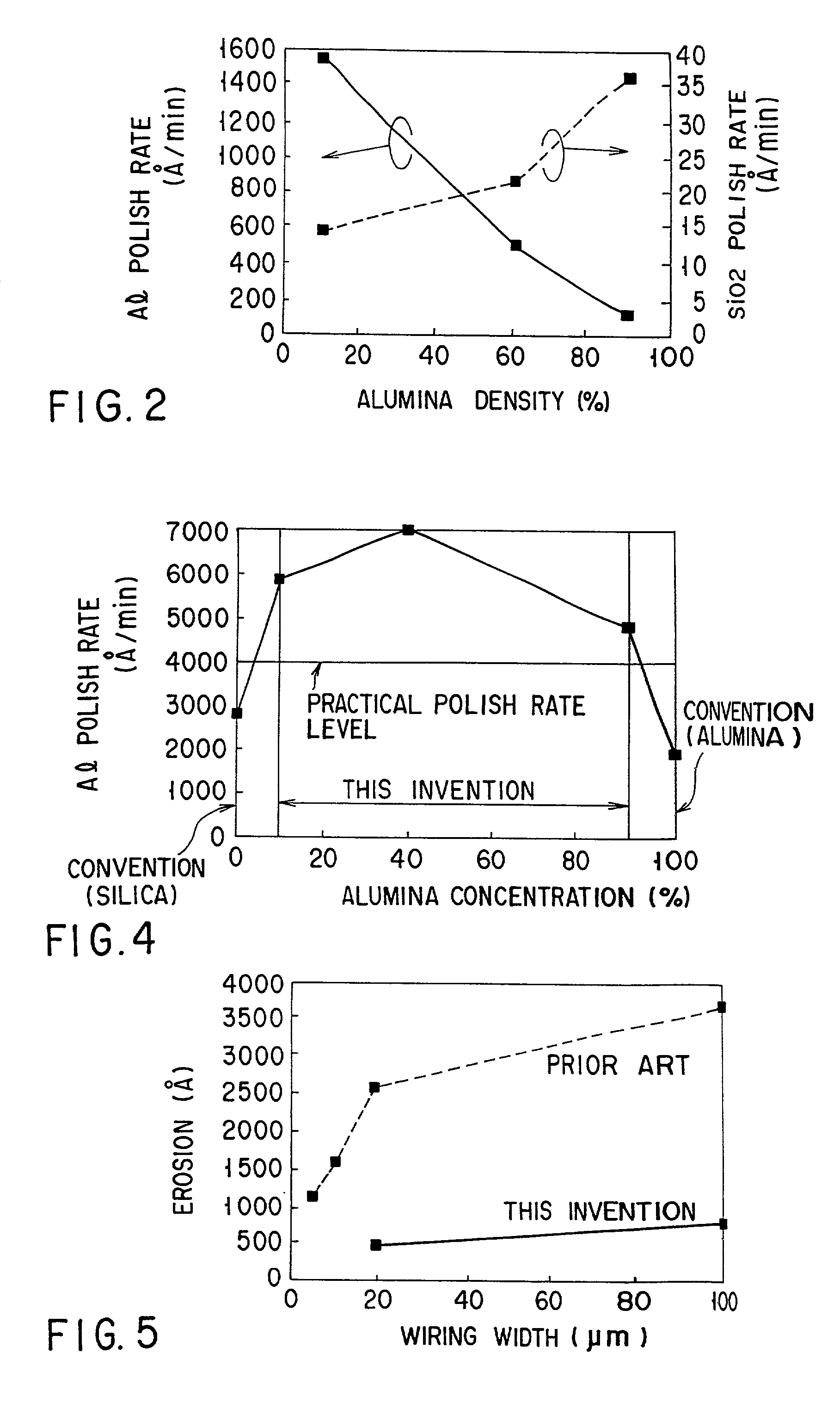
[0031]Using the slurry according to the present embodiment, selectivity of the Al film to SiO2 film (Al polishing rat...
second embodiment
[0036]FIGS. 3A to 3D are cross-sectional views illustrating steps of a process of forming Al Damascene wiring according to a second embodiment of the present invention. This embodiment is directed to a method of forming Al Damascene wiring, in which an Nb film is used as a liner film.
[0037]As is shown in FIG. 3A, an SOG (Spin on Glass) film 12 is deposited as an interlayer insulating film on a silicon substrate 11. A wiring trench 13 is formed in a surface portion of the SOG film 12. The steps thus far are common to the first embodiment, except for the kind of the interlayer insulating film.
[0038]As is shown in FIG. 3B, an Nb liner film 14 with a thickness of 30 nm is deposited over an entire surface of the resultant structure. Then, an Al film 15 with a thickness of 600 nm for filling the wiring trench 13 is deposited on the Nb liner film 14.
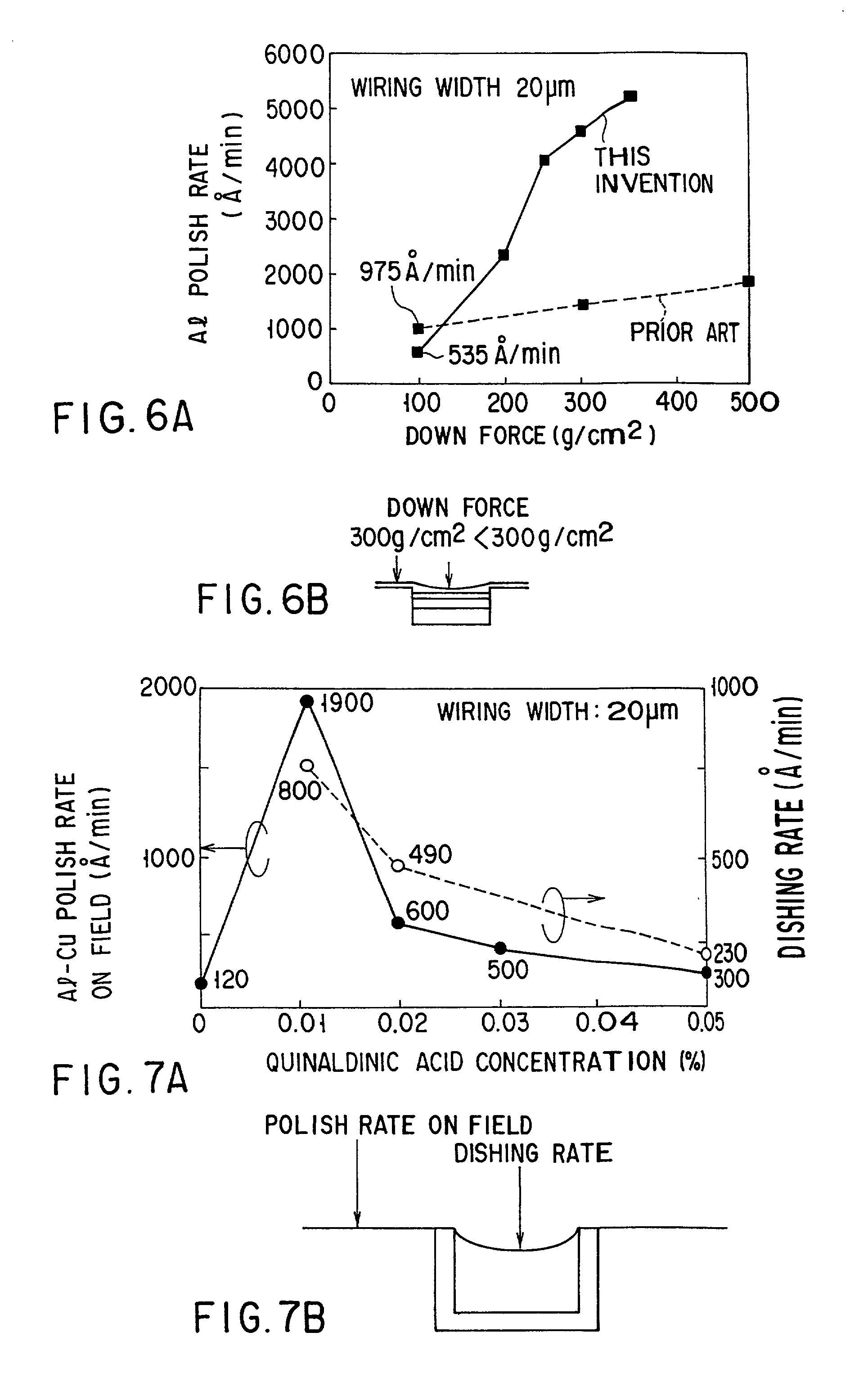
[0039]In a subsequent step, as illustrated in step 3C, the Al film 15 is polished by CMP until the surface of the Nb liner film 14 appears, us...
third embodiment
[0055]FIGS. 8A to 8D are cross-sectional views illustrating steps of a process of forming W Damascene wiring according to a third embodiment of the invention.
[0056]To start with, as shown in FIG. 8A, an SiO2 film 22 which serves as an interlayer insulating film is deposited on a silicon substrate 21 on which devices (not shown) are fabricated. A wiring trench 23 is then formed in a surface portion of the SiO2 film 22.
[0057]As is shown in FIG. 8B, a Ti liner film 24 with a thickness of 30 nm is deposited over an entire surface of the resultant structure. Then, a TiN liner film 25 is formed over a surface of the Ti liner 24 by a nitriding anneal process at 500° C. A W film 26 for filling the inside of the wiring trench 23 is deposited on the TiN liner film 25.
[0058]Subsequently, as illustrated in FIG. 8C, the W film 26 is polished by CMP until the surface of the TiN liner film 25 appears, using a slurry containing 3% of hydrogen peroxide as an oxidizing agent, 3% of succinic acid as a...
PUM
| Property | Measurement | Unit |
|---|---|---|
| thickness | aaaaa | aaaaa |
| pH | aaaaa | aaaaa |
| thickness | aaaaa | aaaaa |
Abstract
Description
Claims
Application Information
 - R&D
- Intellectual Property
- Life Sciences
- Materials
- Tech Scout
- Unparalleled Data Quality
- Higher Quality Content
- 60% Fewer Hallucinations
Browse by: Latest US Patents, China's latest patents, Technical Efficacy Thesaurus, Application Domain, Technology Topic, Popular Technical Reports.
© 2025 PatSnap. All rights reserved.Legal|Privacy policy|Modern Slavery Act Transparency Statement|Sitemap|About US| Contact US: help@patsnap.com


