
Piezoelectric actuator array and manufacturing method

a piezoelectric actuator and manufacturing method technology, applied in the field of piezoelectric actuator arrays, can solve the problems of increased device dimensions (width or thickness), natural and inevitable increase of device dimension, and increased generation force, etc., to achieve large displacement, reduce voltage, and reduce the effect of generation for

Inactive Publication Date: 2008-03-11
NGK INSULATORS LTD
View PDF4 Cites 3 Cited by
  • Summary
  • Abstract
  • Description
  • Claims
  • Application Information

AI Technical Summary

Benefits of technology

[0017]As described above, there has been a demand for a piezoelectric actuator in which a generated displacement is consistent with a generation force and which can independently be disposed in a ultrahigh density, but the piezoelectric actuator has not heretofore been proposed. The present invention has been developed to meet this demand. That is, an object of the present invention is to provide a piezoelectric actuator which can obtain a large displacement with a lower voltage and whose generation force is large and which is superior in mounting properties and which can highly be integrated, and to provide a manufacturing method of the piezoelectric actuator. Further object is to apply the piezoelectric actuator in optical micro-devices such as an optical switch, optical shutter, and mirror array, an image display apparatus, a high-frequency filter, a micro-pump, a droplet discharge apparatus, and the like so that capabilities of these are enhanced.
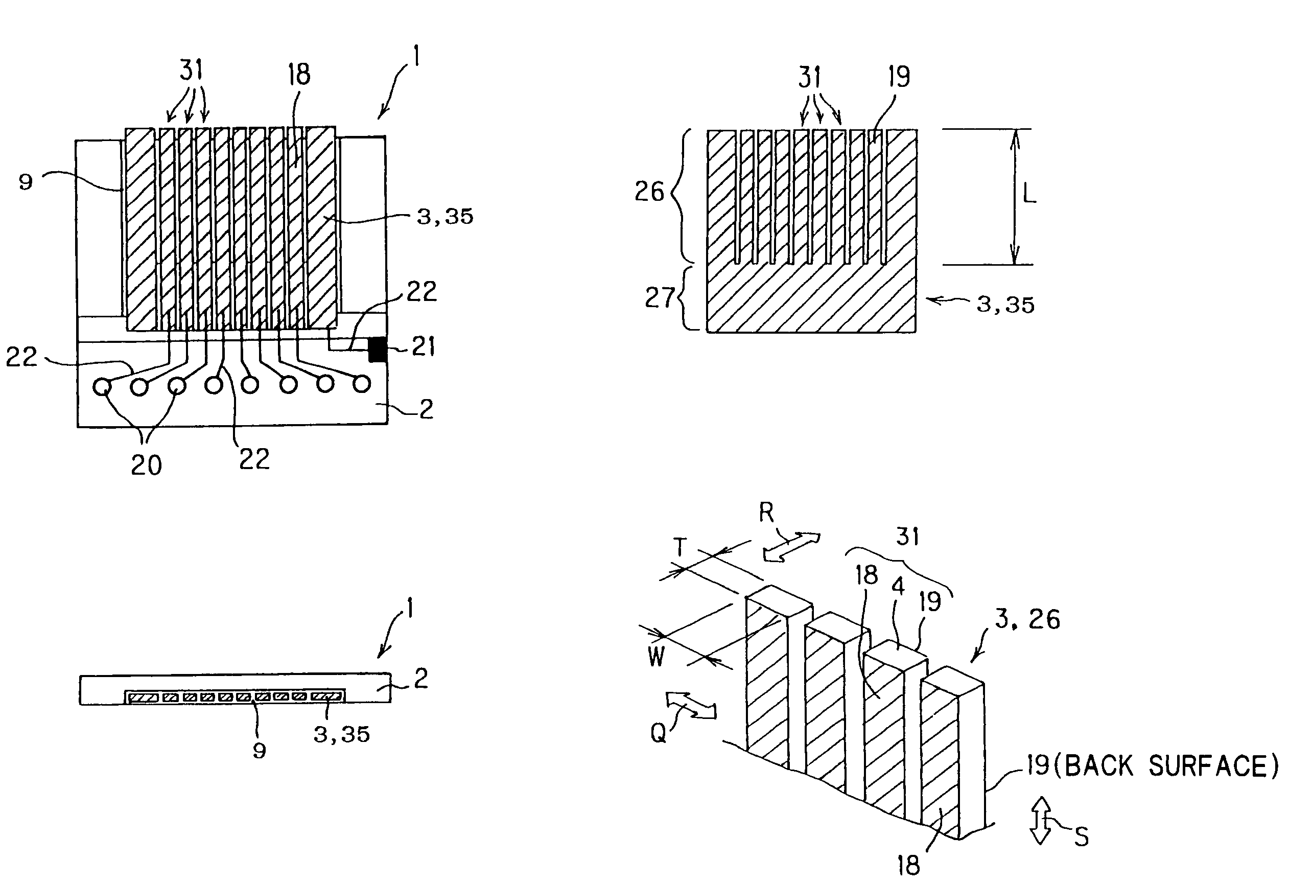
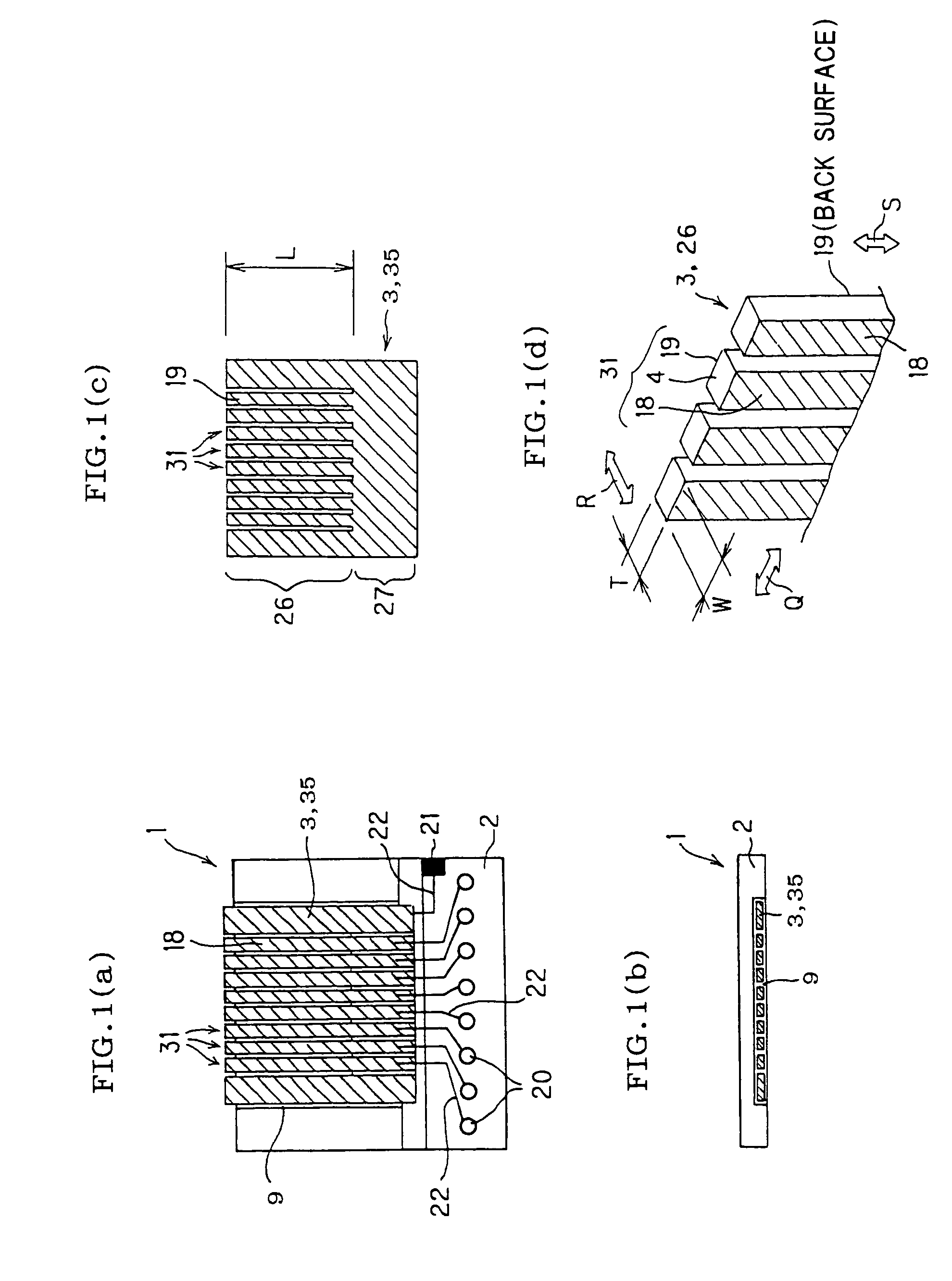
[0020]First, there is provided a one-dimensional piezoelectric actuator array comprising: a piezoelectric device which comprises a plate or pillar-shaped piezoelectric member, and at least one pair of electrodes formed on the piezoelectric member; said piezoelectric device being driven based on a piezoelectric effect of the piezoelectric member and being disposed in a planar form, wherein the piezoelectric device constitutes a piezoelectric device substrate, it is formed in a planar comb shape as a whole in which comb teeth are connected to one another in one end, and comb-teeth portions thus formed are functioned as a plurality of driving portions to, wherein a guide substrate having a concave portion for housing at least a part of the piezoelectric device substrate in a predetermined position in a unified form is further disposed in addition to the piezoelectric device substrate, and the guide substrate and the piezoelectric device substrate are integrally unified in such a manner that the resultant is easily stuck in a multiply stuck structural body (hereinafter sometimes referred to as an arrayed piezoelectric actuator).
[0022]Moreover, to apply a voltage to the piezoelectric member, a wiring circuit connected to a pair of electrodes may also be disposed in a substrate (component) separate from the guide substrate, but is preferably disposed in the guide substrate. Since this structure further becomes simple and is easily prepared, cost can be reduced, and yield can be enhanced.
[0033]Moreover, according to the present invention, there is provided a one-dimensional piezoelectric actuator array comprising: a plurality of piezoelectric devices each of which comprises a plate or pillar-shaped piezoelectric member, and at least one pair of electrodes formed on the piezoelectric member; said constitute a piezoelectric device substrate being driven based on a piezoelectric effect of the piezoelectric member and being disposed in a planar form, wherein a plurality of piezoelectric devices are arranged in the planar form in an independently separated state, in addition to the piezoelectric devices a guide substrate is further disposed a concave portion for housing at least a part of each of the plurality of piezoelectric devices is in a predetermined position in a unified form, and wherein the guide substrate and the plurality of piezoelectric devices are integrally unified in such a manner that the resultant is easily usable to stack it multiply to form a multiply stuck structural body.
[0036]The straightness and axial line described in the present specification are described in Japanese Industrial Standards B0621 “Definition and Display of Geometric Deviation”. The straightness indicates the size of deviation of a linear member from a geometrically correct straight line. The axial line indicates a line which connects centers of sectional contour lines in transverse sections to each other of an object designated as if the linear member were cylindrical or rectangular parallelepiped. In the piezoelectric actuator array according to the present invention, the straightness of the axial line of the driving portion (piezoelectric member) of the piezoelectric device substantially having a substantially pillar shape or mostly having an elongated rectangular parallelepiped shape can be maintained to be remarkably small. This means that the driving portion (piezoelectric member) of the piezoelectric device of the piezoelectric actuator array according to the present invention has a shape remarkably close to the geometrically correct rectangular parallelepiped shape having no deformation such as warpage or bend even when the aspect ratio is large.

Problems solved by technology

However, since the strain is converted, a generated stress applied to the directly generated strain of the piezoelectric device cannot be used as such.
It is very difficult to enlarge the generation force simultaneously with the displacement.
Therefore, a device dimension (width or thickness) naturally and inevitably increases, and it is therefore difficult to dispose the device in a high density while reducing the pitch.
A layer structure including the electrode-piezoelectric member of each independently separated piezoelectric device easily becomes uneven, and there is a problem that fluctuations of characteristics are caused among the devices.
Additionally, considering from the sintering strain, the device dimension (width or thickness) naturally and inevitably increases, and it is therefore difficult to reduce the pitch.
However, this cannot easily be said to be a sufficient integration for handing a resolution which has been required for an ink jet printer in recent years.
Next, in the disclosed piezoelectric actuator, the independently separated piezoelectric devices are formed by the dicing saw processing, but there is a problem that a depth of the groove, that is, a height of the piezoelectric device is inevitably reduced / limited by processing restrictions.
For a lateral effect device in which the generated displacement depends on the height of the piezoelectric device, when the height is limited, the obtained displacement is not sufficient.

Method used


Image

  • Piezoelectric actuator array and manufacturing method
  • Piezoelectric actuator array and manufacturing method
  • Piezoelectric actuator array and manufacturing method

Examples


examples

[0230]The present invention will be described hereinafter based on examples, but the present invention is not limited to these examples.

[0231](Preparation of Piezoelectric Device Substrate)

[0232]A ceramic green sheet formed of a lead zirconate titanate-based ceramic and an organic binder was prepared using a doctor blade method. The thickness of the ceramic green sheet was set to about 200 μm. The ceramic green sheet was sintered at about 1300° C. to prepare the piezoelectric sheet having the flat plate shape. Next, film electrodes were formed as a whole in the opposite surfaces of the piezoelectric sheet. After screen-printing a gold paste, the electrodes were sintered at about 600° C. and formed. Next, this piezoelectric sheet was processed in the comb shape by the mechanical processing using a dicing saw and wire saw. For the comb shape, the pitch of the comb teeth was set to 500 μm, a comb width was 400 μm, and comb length was 15 mm. Next, groove processing was carried out among...


PUM

PropertyMeasurementUnit
widthaaaaaaaaaa
widthaaaaaaaaaa
displacementaaaaaaaaaa

Abstract

There is disclosed a one-dimensional piezoelectric actuator array 1 houses a piezoelectric device 35 including a plate or pillar-shaped piezoelectric member 4 and electrodes 18, 19, and having a planar form; the device 35 being driven by a piezoelectric effect of the piezoelectric member 4. The piezoelectric device 35 is formed as a whole in a planar comb shape wherein comb teeth 26 are connected to one another in one end, and portions of the comb teeth 26 work as a plurality of driving portions 31. The guide substrate 2 and piezoelectric device substrate 3 are integrally unified in such a manner that the resultant is readily usable for the formation of a multiply stuck structural body. In case of need, the array may be further provided with a guide substrate 2 having a concave portion 9 for housing at least a part of the piezoelectric device substrate 3.

Description

BACKGROUND OF THE INVENTION[0001]1. Field of the Invention[0002]The present invention relates to an actuator array which causes displacement based on an electric / mechanic energy conversion using an electric field induced strain such as an inverse piezoelectric effect. In more detail, the present invention relates to a piezoelectric actuator array which is preferably used in an optical switch, optical shutter, optical micro-device such as a mirror array, image display apparatus, high frequency filter, micro-pump, droplet discharge apparatus, and the like and which achieves both a high generation force and large displacement and in which a piezoelectric member causing the displacement has a high aspect ratio superior in consistency of the generation force and displacement and which is easily handled and positioned, and also relates to a manufacturing method of the actuator array.[0003]2. Description of the Related Art[0004]In recent years, in an optical field, precision machine field,...

Claims


Application Information

Patent Timeline
Patent Type & Authority Patents(United States)
IPC IPC(8): H01L41/08B81B3/00B81B7/04B81C3/00G02B6/35G02B26/08H01L27/20H01L41/053H01L41/083H01L41/09H01L41/187H01L41/193H01L41/22H01L41/313H01L41/339H02N2/00
CPCB81B7/04B81C3/002G02B6/3578G02B26/0858H01L27/20H01L41/053B81B2201/038G02B6/3502G02B6/3514G02B6/3544H10N39/00H10N30/88
Inventor KAWAGUCHI, TATSUOKIMURA, KOJI
Owner NGK INSULATORS LTD
Learn More