High-speed differential logic to CMOS translator architecture with low data-dependent jitter and duty cycle distortion

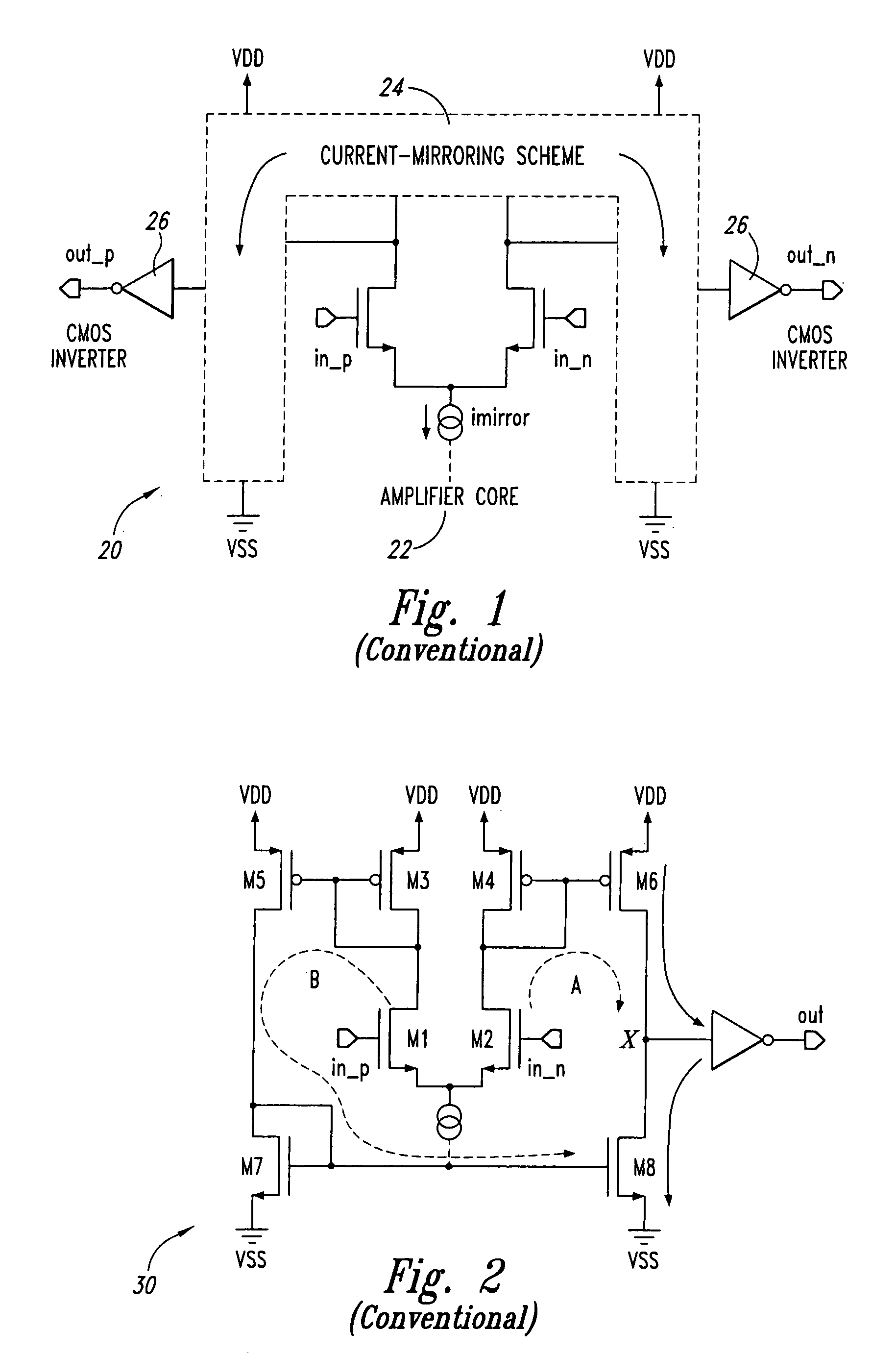
a translator and differential logic technology, applied in logic circuits, pulse automatic control, pulse techniques, etc., can solve the problems of low data-dependent jitter and duty cycle distortion of cmos translators, reducing circuit bandwidth, and node x is a high-impedance node, so as to reduce the skew of any signal received and reduce the skew of signals

Active Publication Date: 2007-11-27
MONTEREY RES LLC
View PDF16 Cites 16 Cited by
  • Summary
  • Abstract
  • Description
  • Claims
  • Application Information

AI Technical Summary

Benefits of technology

[0011]According to another aspect of the embodiment, a method of translating a differential logic signal to a CMOS logic signal includes level-shifting and buffering differential input signals to provide resulting signals with lower common mode voltage. The method also includes using a gain stage to provide increased swing signals from the resulting lower common mode signals and using a CMOS buffer to provide a CMOS output from the increased swing signals. The method may also include reducing signal skew within the CMOS buffer.
[0015]In one example, the pull-down path may include a first transistor and a second transistor connected in series, the first transistor coupled between a supply voltage and the second transistor, the second transistor coupled between ground and the first transistor, both the first and second transistors controlled by the first of the set of increased swing signals. The pull-up path may include a third transistor and a fourth transistor connected in series, the third transistor coupled between a supply voltage and the fourth transistor, the fourth transistor coupled between ground and the third transistor. Further, the translator may include means for reducing any signal skew received by or within the CMOS buffer.
[0016]According to another broad aspect of another embodiment of the present invention, disclosed herein is an integrated circuit having at least one set differential logic signals; and a translator for translating the at least one set of differential logic signals into a CMOS logic signal. In one example, the translator may include a buffering and level shifting stage configured to receive the at least one set of differential logic signals and to provide a first output; a gain stage coupled with the first output and providing a second output; and a CMOS buffer stage coupled with the second output and providing the CMOS logic signal. The CMOS buffer stage of the translator may include means for reducing signal skew within the CMOS buffer.

Problems solved by technology

One such disadvantage is that unequal current switching paths can lead to jitter in timing.
However, most such approaches add devices to the circuit.
Adding more devices to equalize the current paths can lead to additional capacitance in the circuit, thus decreasing the circuit's bandwidth.
Another disadvantage is that node x is a high-impedance node, due to the saturation resistances of transistors M6 and M8, which are generally large.
This means that slight changes in current through those two transistors can lead to large voltage changes at node x. In turn, the voltage at node x is not well controlled.
Mismatch between transistors M6 and M8 would also significantly affect the voltage value of node x. Of course, it is impossible to match M6 and M8 over all process corners, which means that node x is, in practice, not well controlled.
Another disadvantage of this conventional approach 30 is that variations in transistor performance over process, voltage, and temperature (PVT) corners can lead to varying jitter performance.
Even if relatively low jitter can be achieved by matching transistors in the amplifier section and in the output inverter for one corner, the matching would no longer be applicable if the transistor silicon performance changed due to process variations or if operating environment parameters changed.

Method used


Image

  • High-speed differential logic to CMOS translator architecture with low data-dependent jitter and duty cycle distortion
  • High-speed differential logic to CMOS translator architecture with low data-dependent jitter and duty cycle distortion
  • High-speed differential logic to CMOS translator architecture with low data-dependent jitter and duty cycle distortion

Examples


Embodiment Construction

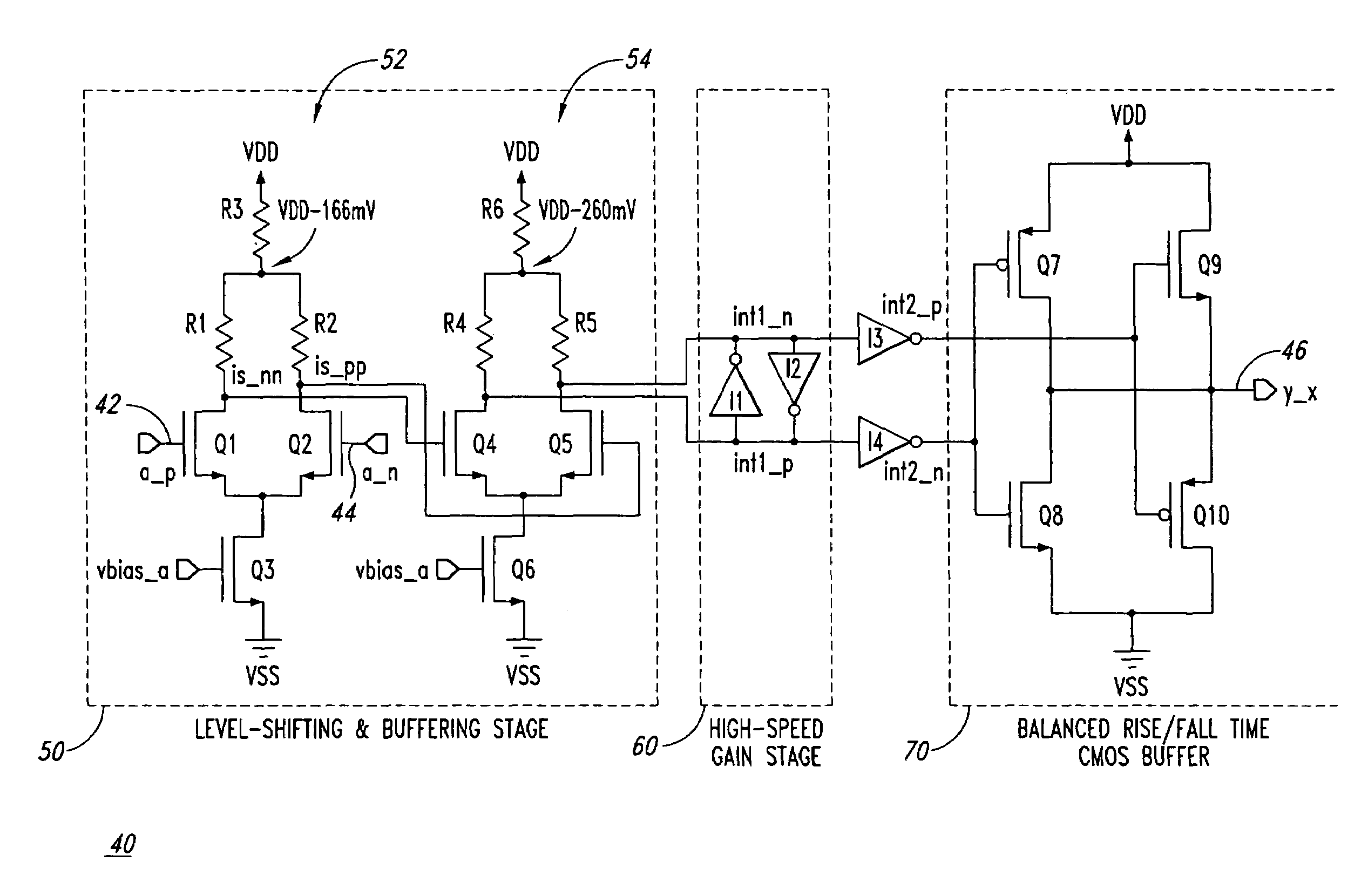
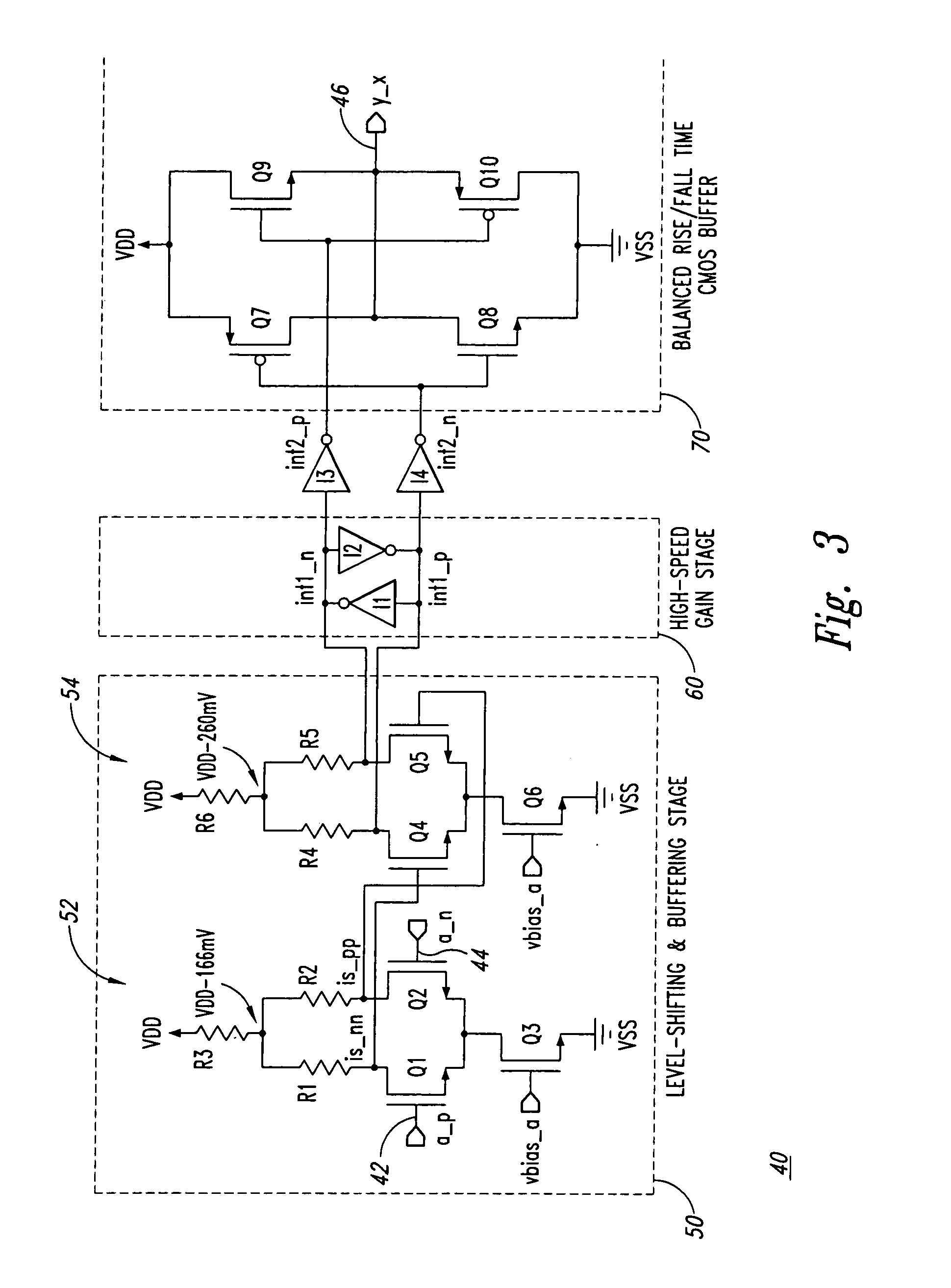
[0022]Disclosed herein is a circuit which can be used as a translator of a differential logic pair of signals into a single ended CMOS logic signal. The circuit can be included in an integrated circuit, such as where high speed data differential logic signals are used. Various embodiments of the present invention are described herein.

[0023]FIG. 3 is a schematic diagram of an improved differential logic to CMOS logic translation circuit 40. In FIG. 3, the inputs are the signals 42, 44 a_p and a_n, and the output 46 is the signal y_x, a single CMOS logic signal instead of a pair of signals. On the input side in the example of FIG. 3, if the voltage on a_p is greater than the voltage on a_n, that represents a logic 1 or logic high; if the voltage on a_n is greater than the voltage on a_p, that represents a logic 0 or logic low. In the example of FIG. 3, if the input signal a_p is greater than a_n (i.e., logic high), then the output signal y_x will be logic high as well. If the input si...


PUM


Abstract

Disclosed are various embodiments of a differential logic to CMOS logic translator including a level-shifting and buffering stage configured to receive differential inputs and to provide resulting signals with lower common mode voltage. Further, a gain stage is included to receive the resulting signals and to provide increased swing signals. A CMOS buffer is also included and is configured to receive the increased swing signals and to provide a CMOS logic output. Also disclosed is a method of translating a differential logic signal to a CMOS logic signal including level-shifting and buffering differential input signals to provide resulting signals with lower common mode voltage. The method also includes using a gain stage to provide increased swing signals from the resulting lower common mode signals and using a CMOS buffer to provide a CMOS output from the increased swing signals.

Description

CROSS REFERENCE TO RELATED APPLICATION[0001]This application claims the benefit under 35 U.S.C. § 119(e) to U.S. Provisional Application No. 60 / 472,973 entitled “A HIGH-SPEED DIFFERENTIAL LOGIC TO CMOS TRANSLATOR ARCHITECTURE WITH LOW DATA-DEPENDENT JITTER AND DUTY CYCLE DISTORTION,” filed May 22, 2003, the disclosure of which is hereby incorporated by reference in its entirety.TECHNICAL FIELD[0002]The present invention relates generally to integrated circuits and, more particularly, to circuitry for translating a differential logic signal to a CMOS logic signal.BACKGROUND OF THE INVENTION[0003]Many chip interfaces use differential signaling, such as Low-Voltage Differential Signaling (LVDS), for high-speed signal transmission such as multi gigahertz applications as an example. However, most internal chip circuit functions are implemented using full CMOS logic type signals. Therefore, translation circuits for converting differential signals into CMOS logic signals are required. In a...

Claims


Application Information

Patent Timeline
Patent Type & Authority Patents(United States)
IPC IPC(8): H03K19/094H03K19/0175
CPCH03K19/0948H03K19/018528
Inventor HANNA, SHERIFLANDRY, GREG J.REFALO, ALANVIJAYARAGHAVAN, JEYENTH
Owner MONTEREY RES LLC
Why Eureka
Try Eureka