Lithographic apparatus, method of manufacturing a device, and device manufactured thereby

a technology of lithographic apparatus and manufacturing method, applied in the direction of photomechanical apparatus, instruments, optics, etc., can solve the problems of significant and unpredictable variations, not all variations in absorption are easily or accurately predictable, and the exposure intensity profile can cross the resist threshold at the wrong point, so as to avoid or alleviate the

Inactive Publication Date: 2007-10-16
ASML NETHERLANDS BV
View PDF16 Cites 0 Cited by
  • Summary
  • Abstract
  • Description
  • Claims
  • Application Information

AI Technical Summary

Benefits of technology

[0016]An object of the present invention is therefore to provide an improved dose sensing and control system which avoids or alleviates the problems of known energy sensors and dose control systems.
[0018]The sensor, which may comprise one or more photodiodes, for example, detects luminescence radiation caused by the interaction of the projection beam radiation, such as ultraviolet radiation, with the material of the projection system, such as calcium fluoride or quartz lens elements. The luminescence radiation intensity is indicative of the dose being delivered to the substrate. Unlike other dose sensors, no part of the projection beam is additionally blocked or diverted, because the luminescence radiation is an intrinsic property of the interaction of the projection beam radiation and the lens. Furthermore, the luminescence radiation can be measured from the projection system very close to the substrate, and therefore, unlike other dose measurements, is not prone to errors due to transmission variations in the optical path from the radiation source to the substrate. The luminescence radiation can be measured at the side of or beyond the end of the projection system and therefore can avoid occupying the very limited space between the projection system and the substrate. In addition, the luminescence given off by the substrate or a layer of material on the substrate can also be measured to determine the dose of radiation reaching the substrate.
[0019]According to one embodiment, the sensor comprises a plurality of detectors. These can capture the luminescence radiation emitted in different directions and can be summed to produce a signal. According to another embodiment, a radiation guide is provided to direct the luminescence radiation emitted in a plurality of directions all to a single detector. This reduces the cost and wiring complexity of a plurality of detectors, and enables the single detector to be located remote from the projection system to reduce the space overhead and to facilitate exchangeability of the detector.
[0022]The projection beam of radiation, such as ultraviolet radiation, interacting with a material at the surface of the substrate, such as on the surface of a semiconductor material and / or a surface of a conductive material, can also lead to formation of free charges, such as electrons. Therefore, one can set up a detector in the vicinity of the substrate to detect the electrons. In this way, the intensity profile of the radiation beam reaching the substrate can be determined.

Problems solved by technology

If the beam intensity is substantially incorrect, the exposure intensity profile can cross the resist threshold at the wrong point.
While the known method of dose control takes account of variations in the output of the radiation source and deals well with predictable variations in absorption downstream of the energy sensor, not all variations in absorption are easily or accurately predictable.
Any variations in the composition of the flushing gas or leaks from the outside can result in significant and unpredictable variations in the absorption of the beam in the downstream parts of the apparatus and hence of the dose delivered to the resist.

Method used


Image

  • Lithographic apparatus, method of manufacturing a device, and device manufactured thereby
  • Lithographic apparatus, method of manufacturing a device, and device manufactured thereby
  • Lithographic apparatus, method of manufacturing a device, and device manufactured thereby

Examples


embodiment 1

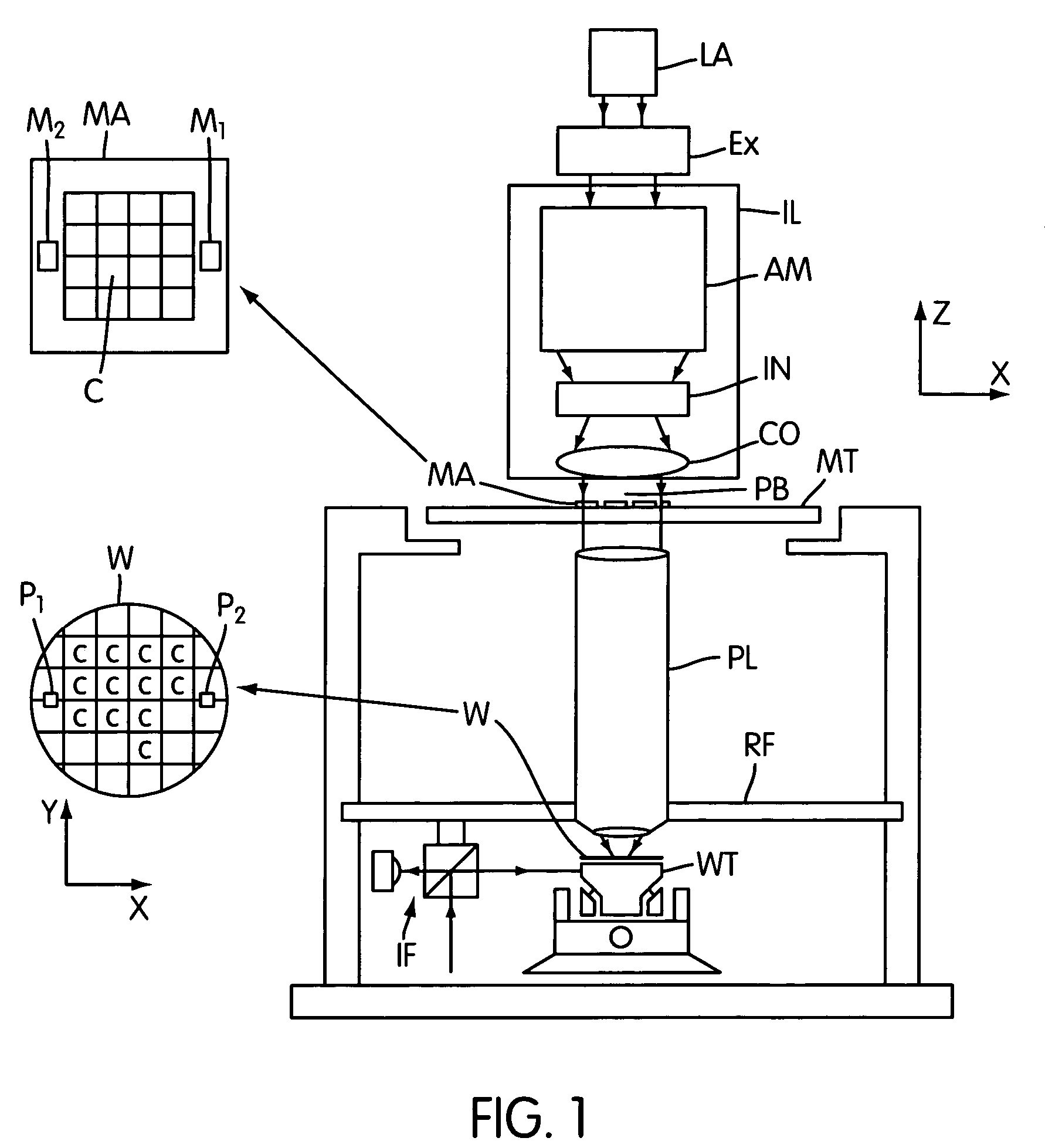
[0036]FIG. 1 schematically depicts a lithographic projection apparatus according to a particular embodiment of the invention. The apparatus comprises: a radiation system LA, Ex, IL, for supplying a projection beam PB of radiation (e.g. UV radiation); a first object table (mask table) MT for holding a mask MA (e.g. a reticle), and connected to first positioning system for accurately positioning the mask with respect to item PL; a second object table (substrate table) WT for holding a substrate W (e.g. a resist-coated silicon wafer), and connected to second positioning system for accurately positioning the substrate with respect to item PL; and a projection system (“lens”) PL (e.g. a quartz and / or CaF2 lens system or a catadioptric system comprising lens elements made from such materials) for imaging an irradiated portion of the mask MA onto a target portion C (comprising one or more dies) of the substrate W. As shown in FIG. 1, mask MA is provided with alignment marks M1 and M2 and s...

embodiment 2

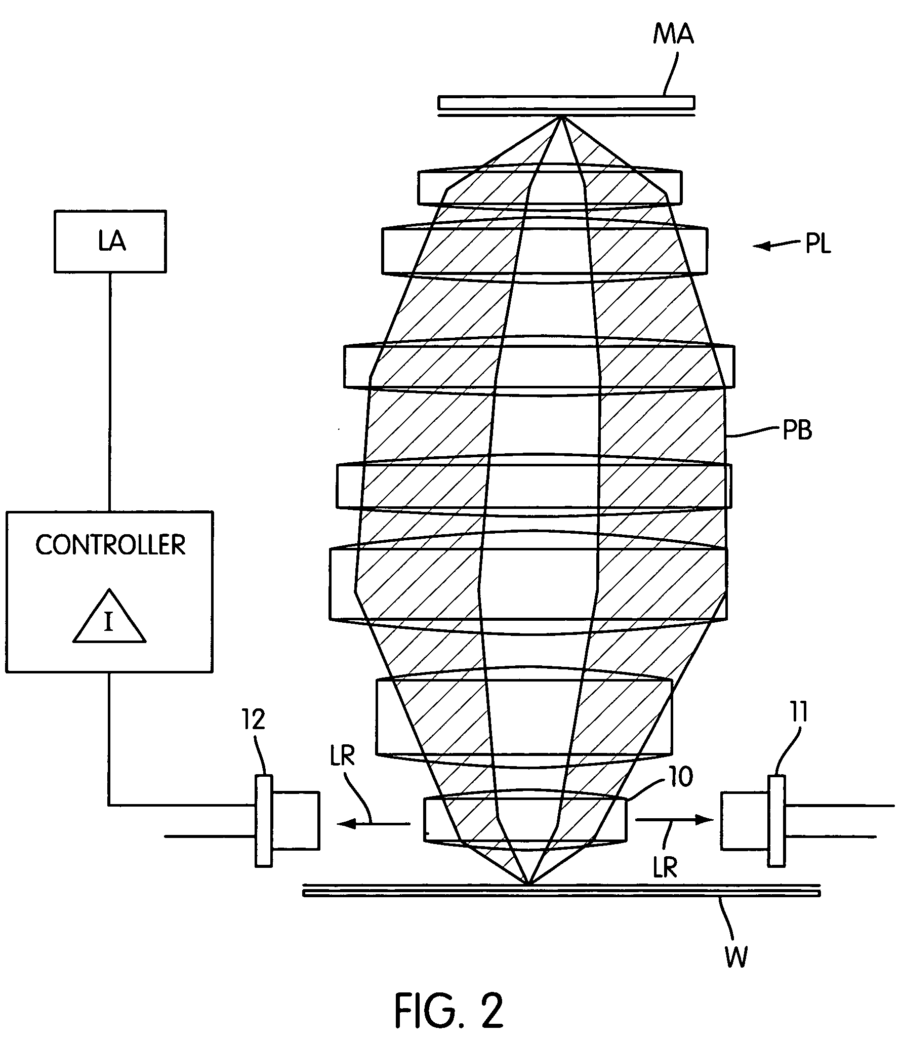
[0047]FIG. 4 shows an arrangement which is essentially the same as that of FIG. 3, except that the detectors have been replaced by reflective elements 30-38 which direct the luminescence radiation to a single detector 39. The inner wall 40 of the projection lens system is also reflective and together with the reflective elements 30-38 forms a reflecting radiation guide. As shown in FIG. 4, one particular reflective element 36 receives luminescence radiation from a wedge-shaped portion 42 of the lens element 10 and reflects it round the radiation guide, as shown by the hatched region 44 to the detector 39. The luminescence radiation directed by all of the other reflective elements has been omitted for clarity, but its path is simply shown by the arrows.

[0048]Other suitable radiation guides can be used, such as optical fibres, to direct the luminescence radiation from different portions of the projection lens element 10 to the single detector 39.

embodiment 3

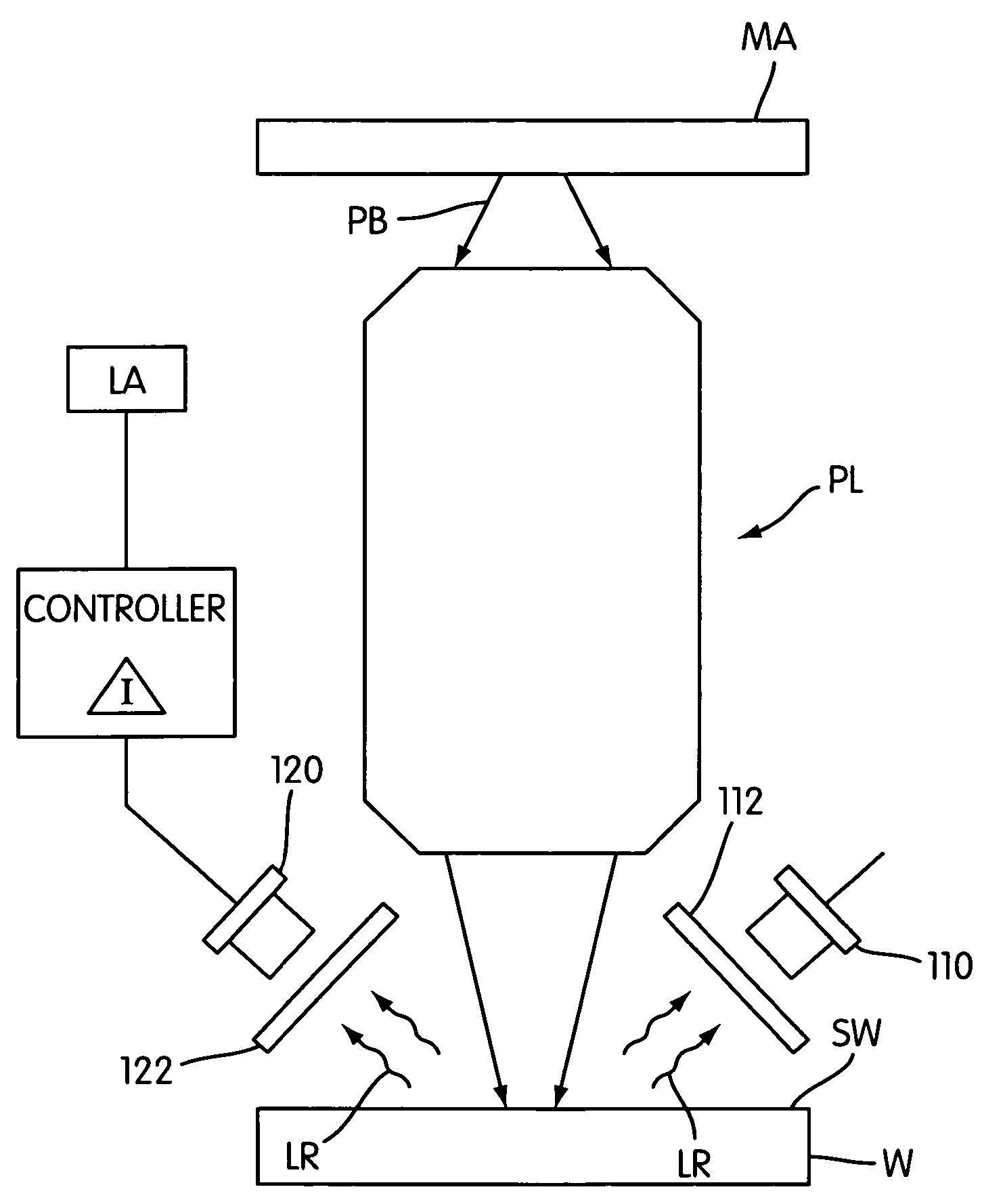
[0049]This embodiment can be the same as the preceding embodiments in all respects except that, as shown in FIG. 5, the luminescence radiation LR from the projection lens element 10 is viewed from outside the lens hood 50, which is incorporated into the machine for gas purging reasons. This simplifies the installation of the luminescence radiation sensor and also improves its subsequent accessibility.

[0050]Although in FIG. 5 detectors 11 and 12 are shown, as in the first embodiment, it is, of course, possible to replace these by a radiation guide and a single detector as in the second embodiment described above.

[0051]In this third embodiment, it will be seen that the luminescence radiation sensor system is located forward of the projection lens element 10 which is closest to the wafer W, rather than being provided in the same plane as the projection lens element 10 as shown in FIGS. 3 and 4. The sensor system detects luminescence radiation emitted from the face of the projection len...


PUM

PropertyMeasurementUnit
wavelengthaaaaaaaaaa
sizeaaaaaaaaaa
sizeaaaaaaaaaa

Abstract

A lithographic projection apparatus is provided with a sensor for detecting one of luminescence radiation, desorbed particles, or free charges produced by an interaction of the projection beam with a material at surface of a substrate. The luminescence radiation, desorbed particles, or free charges are indicative of the dose delivered to the substrate, and can be detected close to the substrate or at the substrate level to avoid errors due to transmission variations in the optical path from the radiation source to the substrate.

Description

[0001]The present Application claims foreign priority under 35 U.S.C. §119(a)-(d) / 365(b) based on EP 01301257.0 filed Feb. 14, 2001, the entire contents of which are incorporated herein by reference. The present Application is a Continuation-in-Part of U.S. patent application Ser. No. 10 / 073,259 filed Feb. 13, 2002 which is now U.S. Pat. No. 6,700,646, the entire contents of which are incorporated herein by reference.BACKGROUND[0002]1. Field of the Invention[0003]The present invention relates to a lithographic projection apparatus comprising a radiation system for supplying a projection beam of radiation; a support structure for supporting patterning component, the patterning component serving to pattern the projection beam according to a desired pattern; a substrate table for holding a substrate; and a projection system for projecting the patterned beam onto a target portion of the substrate.[0004]2. Discussion of Related Art[0005]The term “patterning component” as here employed sh...

Claims


Application Information

Patent Timeline
Patent Type & Authority Patents(United States)
IPC IPC(8): G03B27/72G03B27/42G03F7/20
CPCG03F7/70558
Inventor MULKENS, JOHANNES CATHARINUS HUBERTUSVAN DER VEEN, PAULDE JONGE, ROELSTOLK, ROLAND PIETER
Owner ASML NETHERLANDS BV
Why Eureka
Try Eureka