Method for detection and imaging over a broad spectral range

a detection and imaging technology, applied in the direction of optical radiation measurement, semiconductor/solid-state device details, instruments, etc., can solve the problems of inter-pixel crosstalk, multi-step detector fabrication process, and sophisticated read-out schemes

Inactive Publication Date: 2007-09-25
UCHICAGO ARGONNE LLC +1
View PDF5 Cites 0 Cited by
  • Summary
  • Abstract
  • Description
  • Claims
  • Application Information

AI Technical Summary

Benefits of technology

[0005]This invention represents a departure from traditional detectors of the Focal Plane Array (FPA) design by employing an approach wherein the coordinate sensitivity of a microfabricated superconducting strip is controlled by scanning a beam of energy, such as from a laser or an LCD or in the form of a magnetic field, over the superconducting detector strip so as to physically displace the sensitive area of the detector to permit imaging over a broad spectral range. The superconducting detector strip may either be linear or curvilinear, with the latter equivalent to a two dimensional detector array. In addition to the simplicity of the detector fabrication sequence (one step mask transfer), a clear advantage of this invention is the simplicity of the read-out process: an image is formed by registering the signal with only two electrical terminals. The inventive approach can be extended for imaging over a wide spectral range; the limiting factor being the wavelength-dependent efficiency of thermal conversion in the film / substrate system.
[0007]It is another object of the present invention to provide a method and apparatus for detection and imaging of thermal radiation over a broad wavelength range, i.e., 1 μm-1000 μm, which is commercially feasible and of relatively low cost.
[0008]A further object of the present invention is to control the coordinate sensitivity in a superconducting microbolometer by the application of localized light or magnetic field energy to the detector, or by the use of lithographically defined arrays of micro-heaters in the detector, to simplify the read-out mechanism.
[0010]The present invention is a method of controlling the sensitivity of specific coordinates of a low or high temperature superconducting sensor which provides an IR sensor with broad spectral range sensitivity at relatively low cost. This method can also be applied to control the sensitivity of microbolometers made of other materials that demonstrate sharp dependence of their electrical resistance on temperature or other factors such as magnetic field, etc. Superconducting (SC) films have already been used for various x-ray, infrared, THz, millimeter and microwave applications. Superconducting transition edge sensors have been used as calorimeters and thermistors. The unique property of SC materials is the possibility of utilizing the superconducting, resistive and magnetically ordered phases in the same substance. The type of phases depends on the fabrication methods, and on external effects. SC materials show best performance (with respect to thermal effects) for detection purposes when operating at the critical temperature (Tc), the temperature at which the material becomes superconducting. In this region, even small variations in temperature lead to substantial changes in electrical resistance.
[0011]As an example, we explain the principle of this invention for the case of detection of infrared radiation. However, this same approach can be used for imaging over a broad spectral range (from x-ray to millimeter wavelength). The present invention employs the external action of an optical probe, thermal heating or magnetic field to create normal, superconducting or resistive areas and control their location on the film surface. In other words, once the temperature of the SC film reaches Tc, small changes in the temperature of the film will create large measurable changes in the resistance of the film. Therefore, the invention consists of a superconducting film which may be in the form of a linear or curvilinear strip or a raster-type structure. The image to be detected is optically focused on the surface of the film. The effect of the infrared radiation varies along the strip according to the spatial distribution of the heat source. A laser beam, precisely focused on the SC film is used as an external source of heat to optimally bias the sensor. By adjusting the energy of the laser, the temperature of a specific coordinate on the film can be increased up to Tc to create a local area with optimal response. The laser beam is passed over the film in a raster-like pattern which, when precisely matched with a change in resistance of the film, provides the IR temperature of the image focused on the SC film. Displacement of this resistive (and sensitive to IR radiation) spot along the raster may be used as a basis for a self-scanning image system. Replacement of the strip with a continuous film or curvilinear structure makes two-dimensional imaging possible. In this case, the SC film can include normal, superconducting and transition regions. However, the photo response maximum caused by thermal effects is realized in the transition region. Alternatively, a magnetic field or lithographically defined arrays of micro-heaters or a matrix of light sources (assembly of light emitting diodes, for example) may be used in place of the laser to provide localized, pin-point heating of the SC film. The external action effect can be intensity modulated to increase the signal-to-noise ratio.
[0012]A subtraction of the background contribution (taken with a closed shutter) from IR-produced images can be performed to eliminate any influence of possible sensor defects or surface temperature variation.

Problems solved by technology

The multistep detector fabrication process, inter-pixel crosstalk and sophisticated read-out schemes are common problems in this area of research.

Method used


Image

  • Method for detection and imaging over a broad spectral range
  • Method for detection and imaging over a broad spectral range
  • Method for detection and imaging over a broad spectral range

Examples


Embodiment Construction

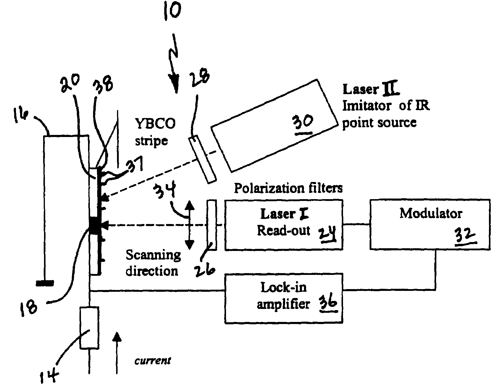
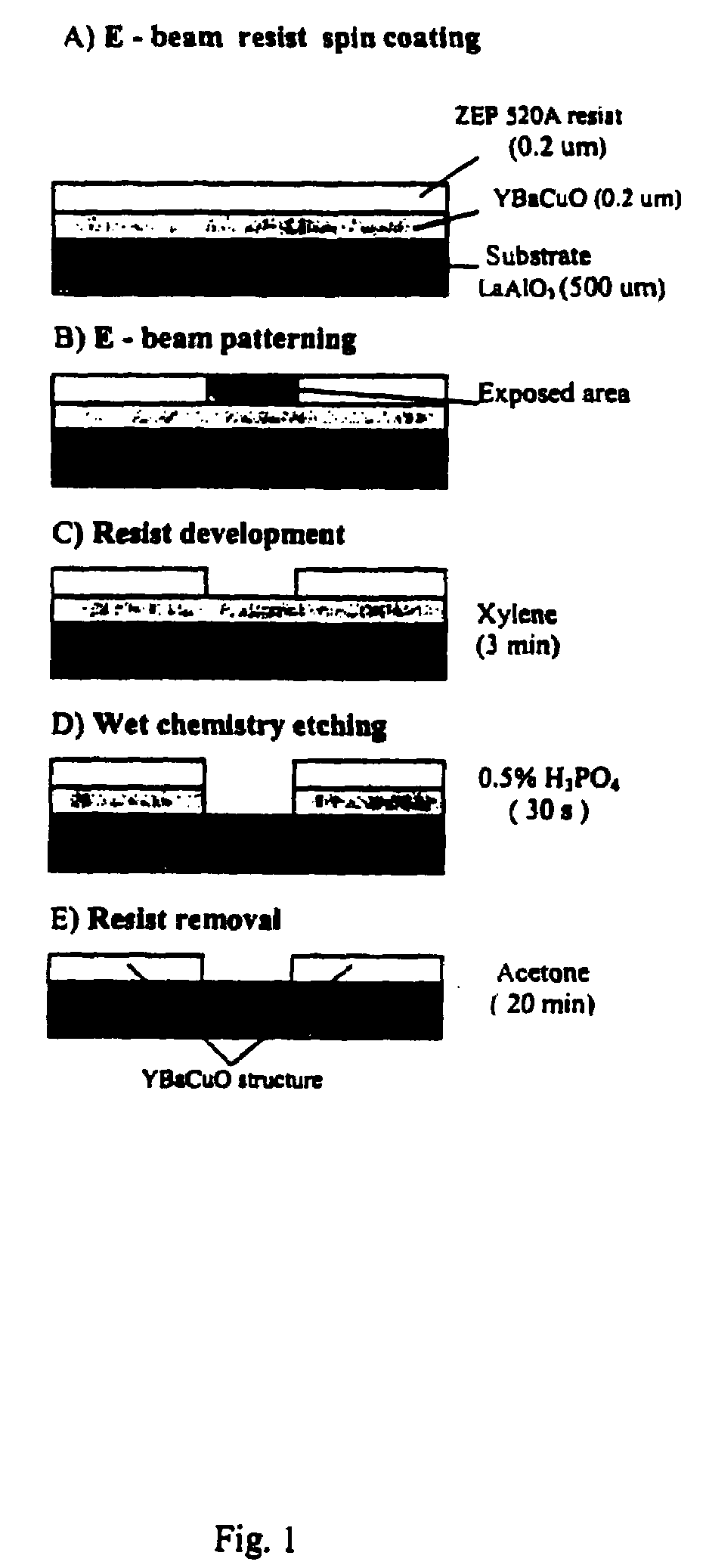
[0021]The detector fabrication sequence is shown in FIG. 1. The HTSC material is a 200 nm thick c-oriented epitaxial Y—Ba—Cu—O (YBCO) film grown on one side of a double-side polished LaAlO3 substrate by laser beam ablation as shown in Step A. The detector geometry is defined by means of electron beam lithography. The thin detector film is spin-coated with a 0.2 μm thick single layer of ZEP-520A resist also applied in Step A. ZEP consists of a copolymer of chloromethscrylate and methalstyrene. ZEP-520A polymer is a high sensitivity e-beam resist of positive tone produced by Nippon Zeon Co. (http: / / www.zeon.co.ip). All exposures are made with a RAITH—Model 150 electron beam system operating at 30 kV with a beam current of 300 pA as shown in Step B. The baking and post-exposure development of the photoresists is performed in Step C according to supplier recommendations. The 40 micron wide and 3 millimeter long stripe-like pattern was then transferred by wet chemical etching in a 0.5% a...


PUM


Abstract

A method of controlling the coordinate sensitivity in a superconducting microbolometer employs localized light, heating or magnetic field effects to form normal or mixed state regions on a superconducting film and to control the spatial location. Electron beam lithography and wet chemical etching were applied as pattern transfer processes in epitaxial Y—Ba—Cu—O films. Two different sensor designs were tested: (i) a 3 millimeter long and 40 micrometer wide stripe and (ii) a 1.25 millimeters long, and 50 micron wide meandering-like structure. Scanning the laser beam along the stripe leads to physical displacement of the sensitive area, and, therefore, may be used as a basis for imaging over a broad spectral range. Forming the superconducting film as a meandering structure provides the equivalent of a two-dimensional detector array. Advantages of this approach are simplicity of detector fabrication, and simplicity of the read-out process requiring only two electrical terminals.

Description

CROSS REFERENCE TO RELATED APPLICATION[0001]This application claims the benefit of U.S. Provisional Application No. 60 / 593,003 filed on Jul. 30, 2004.[0002]The United States Government has rights in this invention pursuant to Contract No. W-31-109-ENG-38 between the U.S. Department of Energy and The University of Chicago representing Argonne National Laboratory.FIELD OF THE INVENTION[0003]This invention relates generally to an improved method and arrangement for detection and imaging over a broad spectral range and is particularly directed to the use of a superconducting film subject to localized, pin-point heating at the critical temperature, Tc, by a laser, magnetic field, micro-heaters, etc.BACKGROUND OF THE INVENTION[0004]The sensitivity of transition edge superconducting (TES) detectors can be comparable to the best liquid nitrogen cooled semiconducting infrared detectors, but with a much larger detection range extending to long wavelengths. Extensive efforts have been directed...

Claims


Application Information

Patent Timeline
Patent Type & Authority Patents(United States)
IPC IPC(8): H01L27/18
CPCG01J5/061G01J5/20G01J2005/0077
Inventor YEFREMENKO, VOLODYMYRGORDIYENKO, EDUARDPISHKO, LEGAL REPRESENTATIVE, OLGANOVOSAD, VALENTYNPISHKO, DECEASED, VITALII
Owner UCHICAGO ARGONNE LLC
Why Eureka
Try Eureka