
Bump electrodes having multiple under ball metallurgy (UBM) layers

a technology of ubm layer and bump electrode, which is applied in the direction of semiconductor/solid-state device details, electrical equipment, semiconductor devices, etc., can solve the problems of shortened device life and degraded device performance, and achieve the effect of prolonging device life and enhancing adhesion between wafer (or chip) and bump electrod

Inactive Publication Date: 2007-09-18
ADVANCED SEMICON ENG INC
View PDF12 Cites 21 Cited by
  • Summary
  • Abstract
  • Description
  • Claims
  • Application Information

AI Technical Summary

Benefits of technology

The present invention provides a wafer structure and a bumping process that enhance adhesion between the wafer and bumps and improve the reliability and quality of the package structure. The wafer structure includes a plurality of bonding pads, a UBM layer, a first passivation layer, and a second passivation layer. The UBM layer includes an adhesion layer, a barrier layer, and a wetting layer. The first metallic layer covers a portion of the first passivation layer and the second passivation layer, providing higher structural strength. The bumping process involves forming bumps on the wafer by sequentially adding layers of metallic and passivation layers. The resultant laminated structure has better connection between the wafer and bump structure, improving the performance and lifespan of the device.

Problems solved by technology

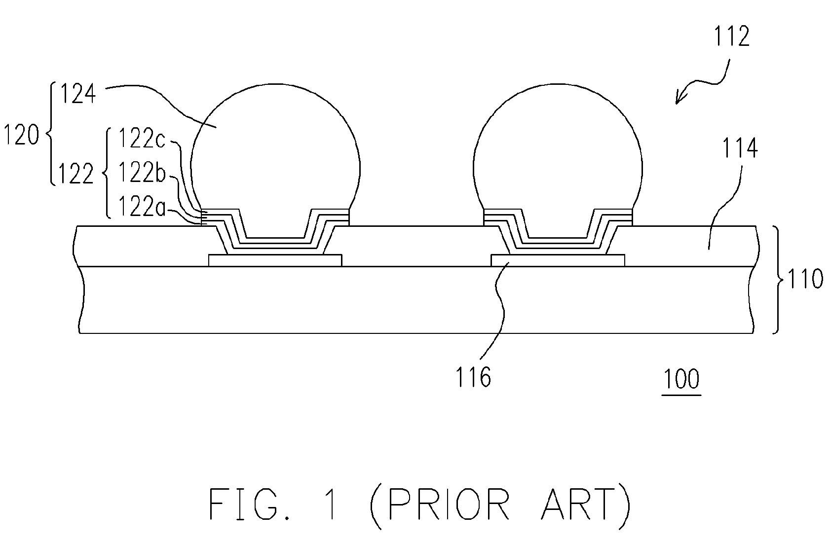
Hence, the performance of the device is degraded and the life of the device is shortened.

Method used


Image

  • Bump electrodes having multiple under ball metallurgy (UBM) layers
  • Bump electrodes having multiple under ball metallurgy (UBM) layers
  • Bump electrodes having multiple under ball metallurgy (UBM) layers

Examples


Embodiment Construction

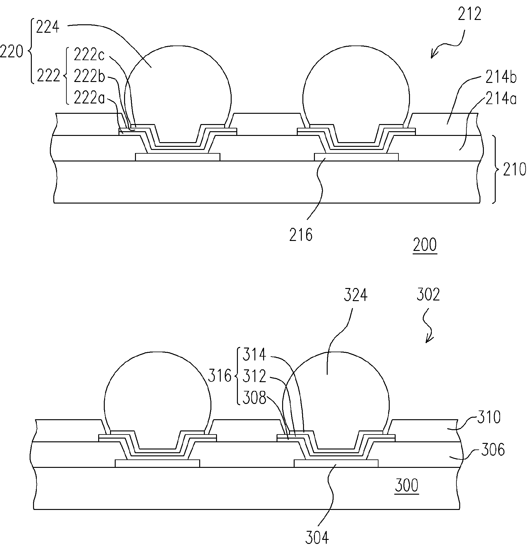
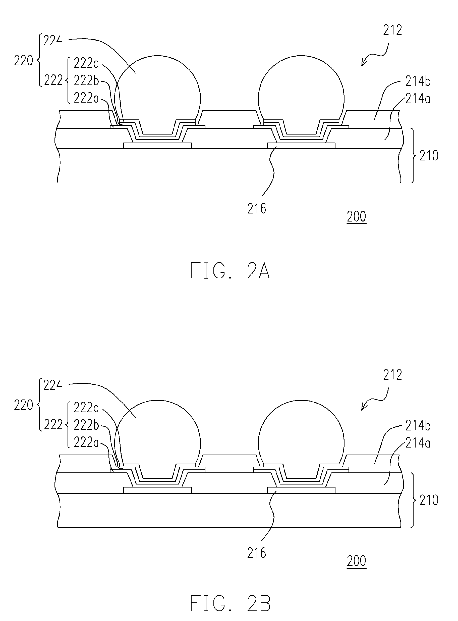
[0024]FIGS. 2A and 2B are cross-sectional display views respectively illustrating two wafer structures according to preferred embodiments of this invention. The same elements in two figures are marked with identical reference numbers.

[0025]Referring to FIG. 2A, the wafer structure 200 includes a wafer 210 and a plurality of bump structures 220 (only two bump structures are shown). The wafer 210 has an active surface 212, a first passivation layer 214a, a second passivation layer 214b, and a plurality of bonding pads 216 (with only two pads shown) on the active surface 212.

[0026]The bonding pads 216 are exposed by the firstpassivation layer 214a, while the first passivation layer 214a covers the active surface 212 of the wafer 210. It is noted that the active surface of the wafer is the surface having active devices of the wafer. The second passivation layer 214b is disposed on the first passivation layer 214a. The material of the second passivation layer 214b can be benzocyclobutene...


PUM


Abstract

The present invention provides a wafer structure having a plurality of bonding pad, an adhesion layer, a barrier layer, a wetting layer, a plurality of bump, a first passivation layer and a second passivation layer. The bonding pads are disposed on the active surface of the wafer and exposed by the first passivation layer. The second passivation layer is disposed on the first passivation layer and exposing the bonding pads. An adhesion layer is disposed on the bonding pad and covers a portion of the first passivation layer. The second passivation layer covers the first passivation layer and a portion of the adhesion layer. The barrier layer and the wetting layer are sequentially disposed on the adhesion layer and the bumps are disposed on the wetting layer.

Description

CROSS REFERENCE TO RELATED APPLICATIONS[0001]This application claims the priority benefit of Taiwan application serial no. 92118830, filed Jul. 10, 2003.BACKGROUND OF INVENTION[0002]1. Field of Invention[0003]The present invention relates to a package structure and the fabrication method thereof. More particularly, the present invention relates to a wafer structure and the bumping process for the wafer structure.[0004]2. Description of Related Art[0005]In the semiconductor industry, integrated circuits (ICs) manufacture can be categorized as three major stages: fabrication of the wafers, fabrication of the ICs and packaging of the ICs. Among the wafer level packaging processes, flip chip (FC) packaging technology has been widely used and become the main stream nowadays. Because FC packaging technology can shorten the signal transmission path between the chip and the substrate, FC packaging technology is suitable for packaging high speed devices, for example, micron or millimeter wav...

Claims


Application Information

Patent Timeline
Patent Type & Authority Patents(United States)
IPC IPC(8): H01L23/488H01L21/44H01L21/60H01L23/485
CPCH01L24/11H01L24/13H01L2224/05027H01L2224/13021H01L2224/131H01L2924/01013H01L2924/01022H01L2924/01029H01L2924/01073H01L2924/01078H01L2924/01082H01L2924/04941H01L2924/04953H01L2924/14H01L2924/0002H01L2224/0401H01L2924/00013H01L2924/01023H01L2924/01033H01L2924/014H01L2224/05572H01L2224/1147H01L2224/13099H01L2224/05552H01L2924/351H01L2224/05124H01L2224/05147H01L2224/05155H01L2224/05166H01L2224/05181H01L2224/05647H01L24/05H01L24/03H01L2924/00H01L2924/00014
Inventor HUANG, MIN-LUNG
Owner ADVANCED SEMICON ENG INC
Learn More