
Method for reducing soft error rates of memory cells

a memory cell and soft error technology, applied in the field of integrated circuit fabrication process and structure, can solve the problems of soft errors, soft errors due to alpha particles becoming more significant, and conventional techniques for dealing with soft errors, such as well engineering, use of n+ or p+ buried layers, or use of epitaxial wafers, are relatively expensive to implement and are not effective in some applications

Active Publication Date: 2007-09-11
INFINEON TECH LLC
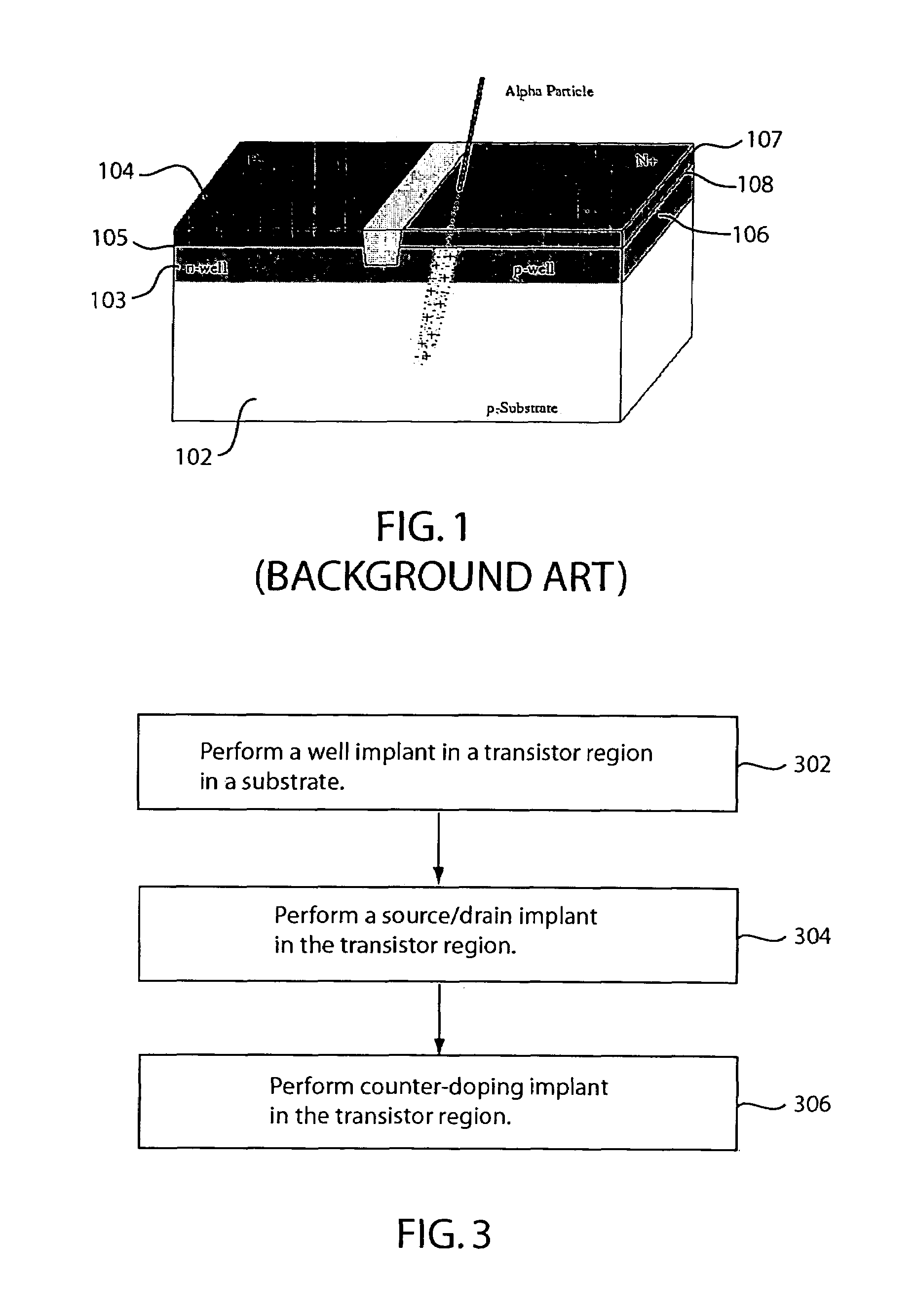
View PDF6 Cites 4 Cited by
  • Summary
  • Abstract
  • Description
  • Claims
  • Application Information

AI Technical Summary

Benefits of technology

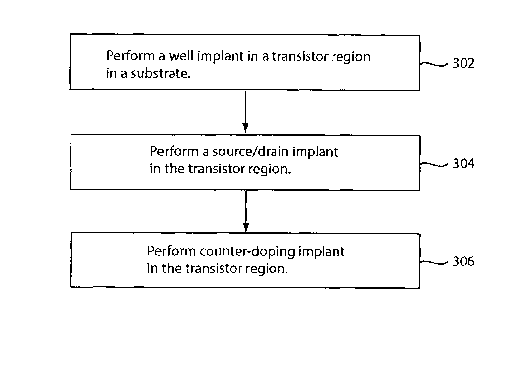
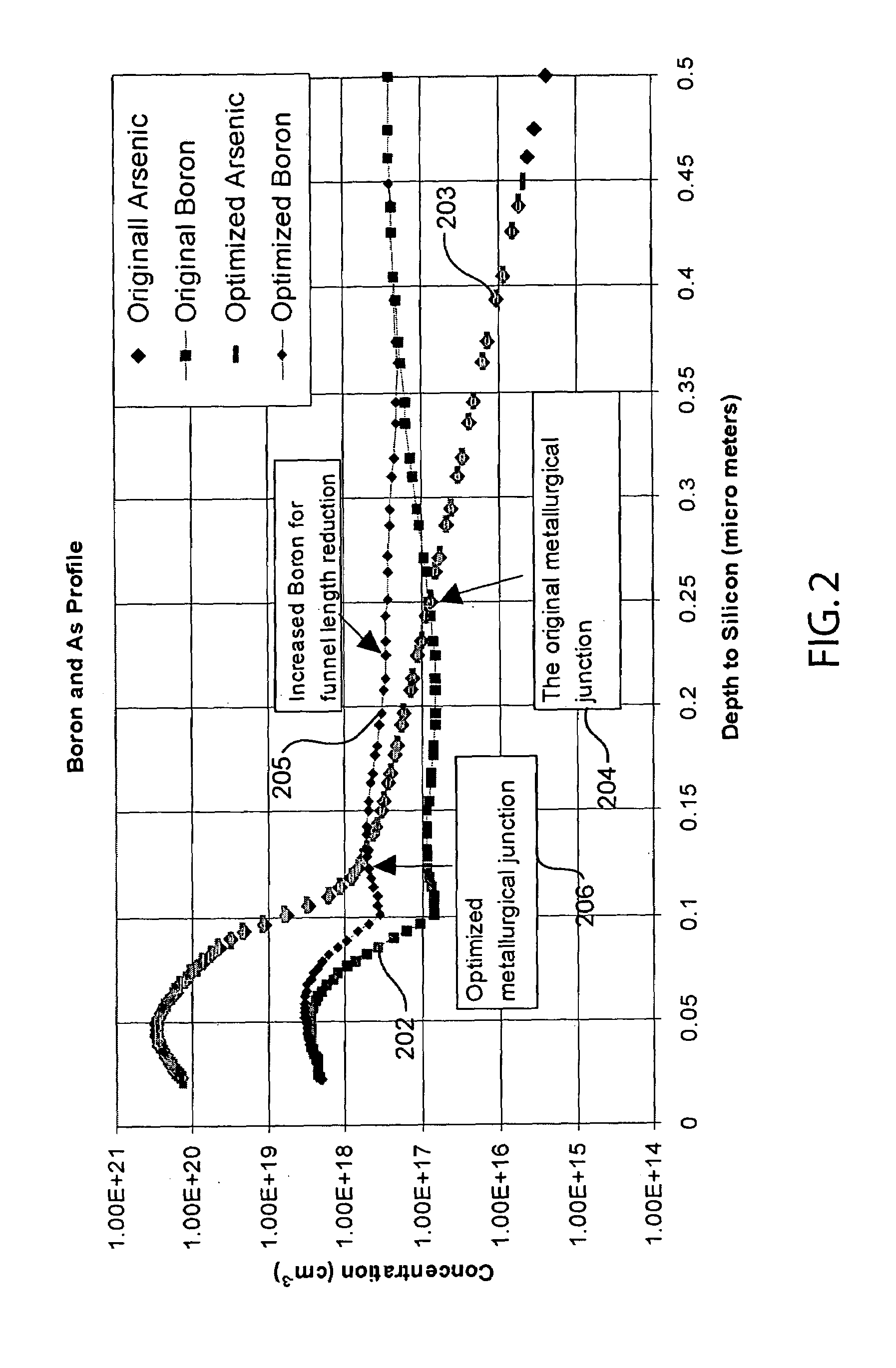
[0008]In one embodiment, a method of fabricating a transistor for a memory cell includes the steps of performing a counter doping implant before or after a source / drain implant. The counter doping implant may comprise one or more implant steps that move a metallurgical junction formed by a well and a highly doped region closer to a surface of the substrate. The counter doping implant may also increase the concentration of the dopant of the well. The counter doping implant and the source / drain implant may be performed using the same mask. Transistors fabricated using embodiments of the present invention may be employed in memory cells to reduce soft error rates.

Problems solved by technology

It is well known that alpha particles can cause soft errors.
Soft errors due to alpha particles become more significant as device geometries shrink.
Unfortunately, conventional techniques for dealing with soft errors, such as implementation of well engineering, use of an N+ or P+ buried layer, or use of an epitaxial wafer, are relatively expensive to implement and are not effective enough in some applications.

Method used


Image

  • Method for reducing soft error rates of memory cells
  • Method for reducing soft error rates of memory cells
  • Method for reducing soft error rates of memory cells

Examples


Embodiment Construction

[0013]In the present disclosure, numerous specific details are provided, such as examples of apparatus, process steps, and structures, to provide a thorough understanding of embodiments of the invention. Persons of ordinary skill in the art will recognize, however, that the invention can be practiced without one or more of the specific details. In other instances, well-known details are not shown or described to avoid obscuring aspects of the invention.

[0014]In one embodiment, memory soft error rates are reduced by counter doping the N+ / P-well junction of an NMOS transistor. The counter-doping implant may comprise a single implant step. The counter doping implant may also comprise multiple implant steps to prevent excessive increase of junction capacitance, which may result in losing contact to the N-well and degradation of junction breakdown voltage.

[0015]In one embodiment, the counter doping implant is performed in conjunction with the source / drain implant. For example, the counte...


PUM


Abstract

In one embodiment, a method of fabricating a transistor for a memory cell includes the steps of performing a counter doping implant before or after a source / drain implant. The counter doping implant may comprise one or more implant steps that move a metallurgical junction formed by a well and a highly doped region closer to a surface of the substrate. The counter doping implant may also increase the concentration of the dopant of the well. The counter doping implant and the source / drain implant may be performed using the same mask. Transistors fabricated using embodiments of the present invention may be employed in memory cells to reduce soft error rates.

Description

REFERENCE TO RELATED APPLICATION[0001]This application claims the benefit of U.S. Provisional Application No. 60 / 505,702, entitled “Method For Improving Soft Error Rates Of Memory Cells,” filed on Sep. 24, 2003 by Yanzhong Xu and Oliver Pohland.BACKGROUND OF THE INVENTION[0002]1. Field of the Invention[0003]The present invention relates generally to integrated circuits, and more particularly to integrated circuit fabrication processes and structures.[0004]2. Description of the Background Art[0005]In the context of memory devices, such as static random access memory (SRAM), a “soft error” is a non-permanent memory error. Most soft errors may be fixed by simply writing new data to the memory. It is well known that alpha particles can cause soft errors. This phenomenon is further described with reference to FIG. 1.[0006]FIG. 1 shows a schematic diagram of a cross-section of a substrate having a P-type metal oxide semiconductor (PMOS) transistor and an N-type metal oxide semiconductor (...

Claims


Application Information

Patent Timeline
Patent Type & Authority Patents(United States)
IPC IPC(8): H01L21/20
CPCH01L21/26513H01L27/11H10B10/00
Inventor XU, YANZHONGPOHLAND, OLIVER
Owner INFINEON TECH LLC
Learn More