
Method for reducing IM2 noise in a down conversion circuit

a conversion circuit and im2 noise technology, applied in the direction of dc level restoring means or bias distort correction, line-faulst/interference reduction, baseband system details, etc., to achieve the effect of reducing current, reducing im2 and dc offset, and relaxing the matching parameters of the mixer

Inactive Publication Date: 2007-08-28
ICERA CANADA ULC
View PDF30 Cites 29 Cited by
  • Summary
  • Abstract
  • Description
  • Claims
  • Application Information

AI Technical Summary

Problems solved by technology

As will be explained, the super-heterodyne's limitations make its use in more sophisticated modern applications expensive, and its performance poor.
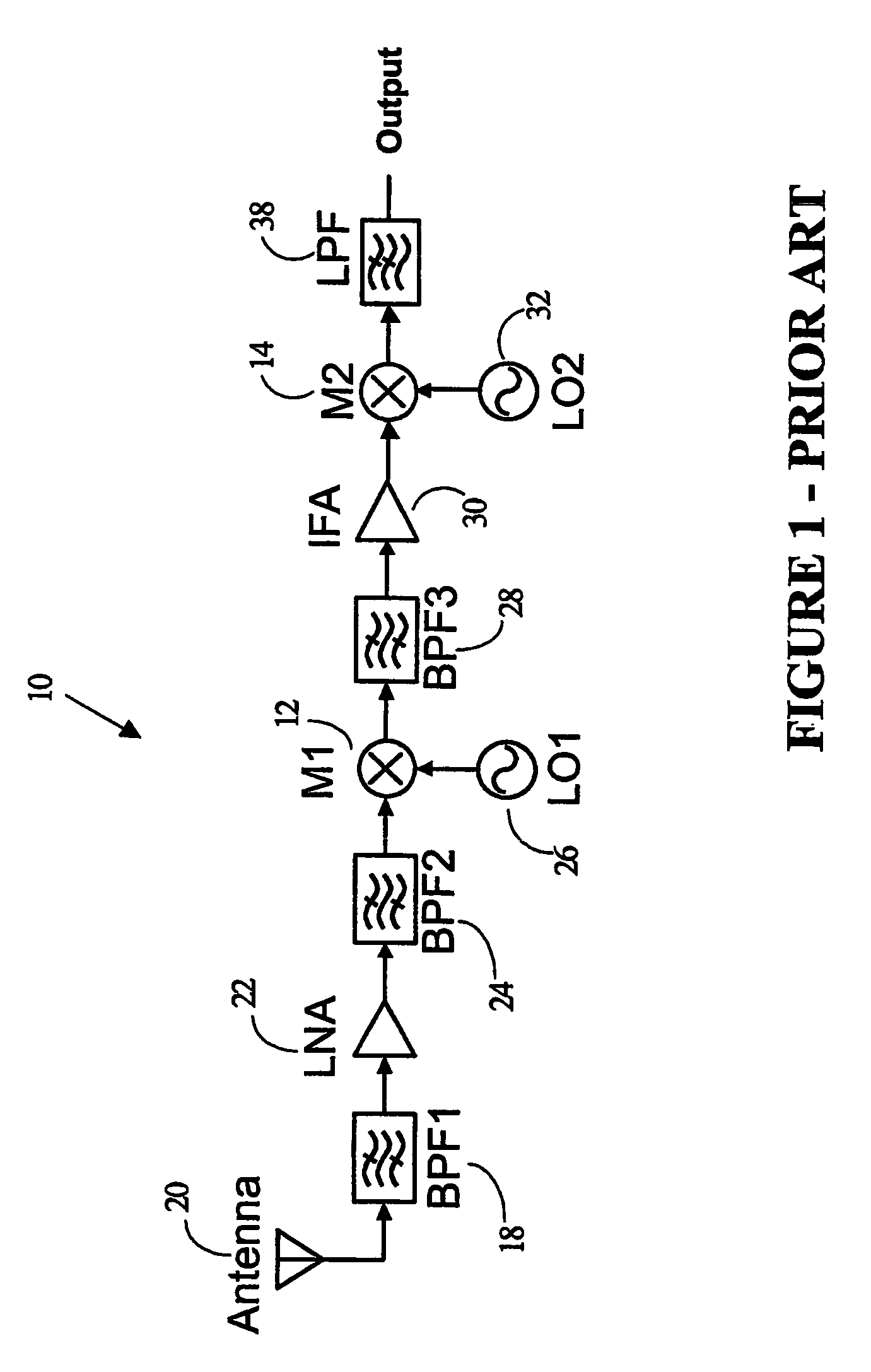
The main problems with the super-heterodyne design are:it requires expensive off-chip components, particularly band pass filters 18, 24, 28, and low pass filter 38;the off-chip components require design trade-offs that increase power consumption and reduce system gain;image rejection is limited by the off-chip components, not by the target integration technology;isolation from digital noise can be a problem; andit is not fully integratable.
However, this technique will generate DC noise signals which interfere with low-frequency information contained in the demodulated baseband signal.
These DC noise signals are particularly difficult to overcome because they are typically unpredictable and time-varying.
Local oscillator (LO) power leaking to the RF input will result in DC levels at the mixer output because it will be mixed with itself.
Hence, there is a potential for large, time-varying DC signals to interfere with the comparatively low-amplitude signals of interest, at or near DC, at the output of the demodulator.
A number of attempts have been made to reduce or compensate for the level of these DC noise signals, but none have been very effective or practical:1. Capacitive CouplingPlacing a capacitor in series with the signal path will block DC noise signals but will also block components of the desired signal near zero frequency.The severity of the data loss is dependent upon the transmission modulation and signal coding.Capacitive coupling also has the disadvantage that the size of the capacitors are generally too large for a fully integrated receiver.2. Adaptive FeedbackDC noise signals may also be removed by the use of adaptive feedback that time-averages the suspected DC offset value and subtracts the corresponding amount from a convenient point along the receive path.
While feedback-based DC-offset reduction techniques are more effective than capacitive coupling and are more easily applied to integrated solutions, the following must be considered when they are applied:a. the increased level of complexity they add to the design;b. since the DC offsets and near DC offsets may be indistinguishable from the desired data, some amount of training time is normally required on a periodic basis to determine the DC offset accurately; andc. if a long-term average of the DC offset is used to estimate how much offset must be subtracted from the input, then this technique will not respond well to rapid variations in the DC offset level; and3. Good Matching of DevicesMis-matching of transistors causes noise and adversely affects performance.The degree of mis-matching increases as component sizes decrease, so performance and yields drop with highly integrated applications.
Neither of these methods are highly effective and of course, result in larger components.
Thus, none of the currently used techniques for addressing the DC noise problem in direct-conversion architectures is particularly effective.
This has proven especially challenging as the frequencies of interest in the wireless telecommunications industry (especially low-power cellular / micro-cellular voice / data personal communications systems) have risen above those used previously (approximately 900 MHz) into the spectrum above 1 GHz.

Method used


Image

  • Method for reducing IM2 noise in a down conversion circuit
  • Method for reducing IM2 noise in a down conversion circuit
  • Method for reducing IM2 noise in a down conversion circuit

Examples


Embodiment Construction

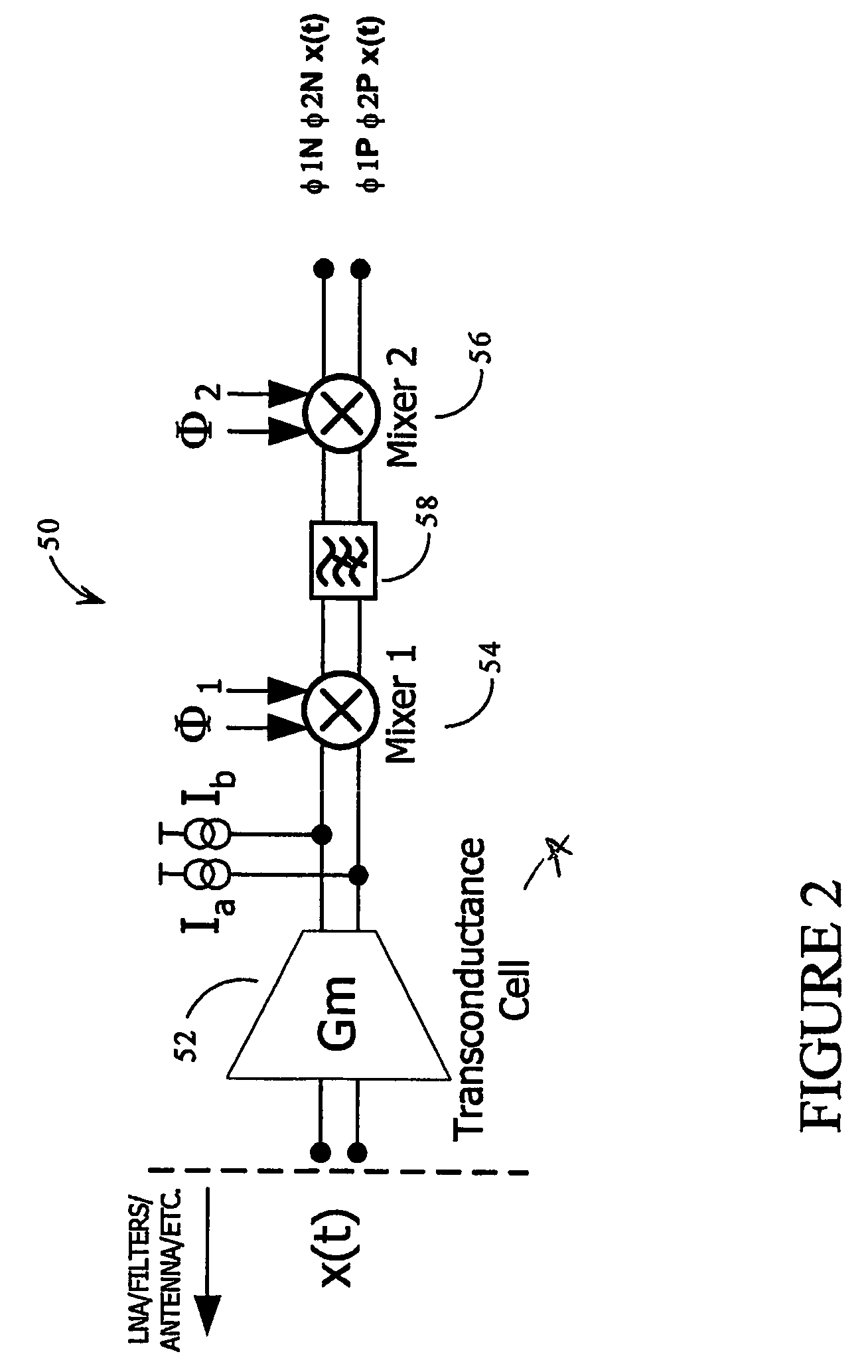
[0060]A circuit which addresses a number of the objects outlined above is presented as a block diagram in FIG. 2. This figure presents a demodulator or down-conversion topology 50 in which a differential input signal x(t) is down-converted by mixing it with two mixing signals φ1 and φ2. A “differential” signal is simply a signal which is available in the form of positive and negative potentials with respect to ground. Thus, this circuit handles an input signal in the form of a differential voltage, x(t)+, x(t)− as the radio frequency (RF) input signal.

[0061]The use of a differential architecture results in a stronger output signal that is more immune to common mode noise than a single ended architecture such as that of FIG. 1. If, for example, environmental noise imposes a noise signal onto the input of FIG. 1, then this noise signal will propagate through the circuit. If the same environment noise is imposed equally on the x(t)+ and x(t)− inputs of the differential circuit of FIG. ...


PUM


Abstract

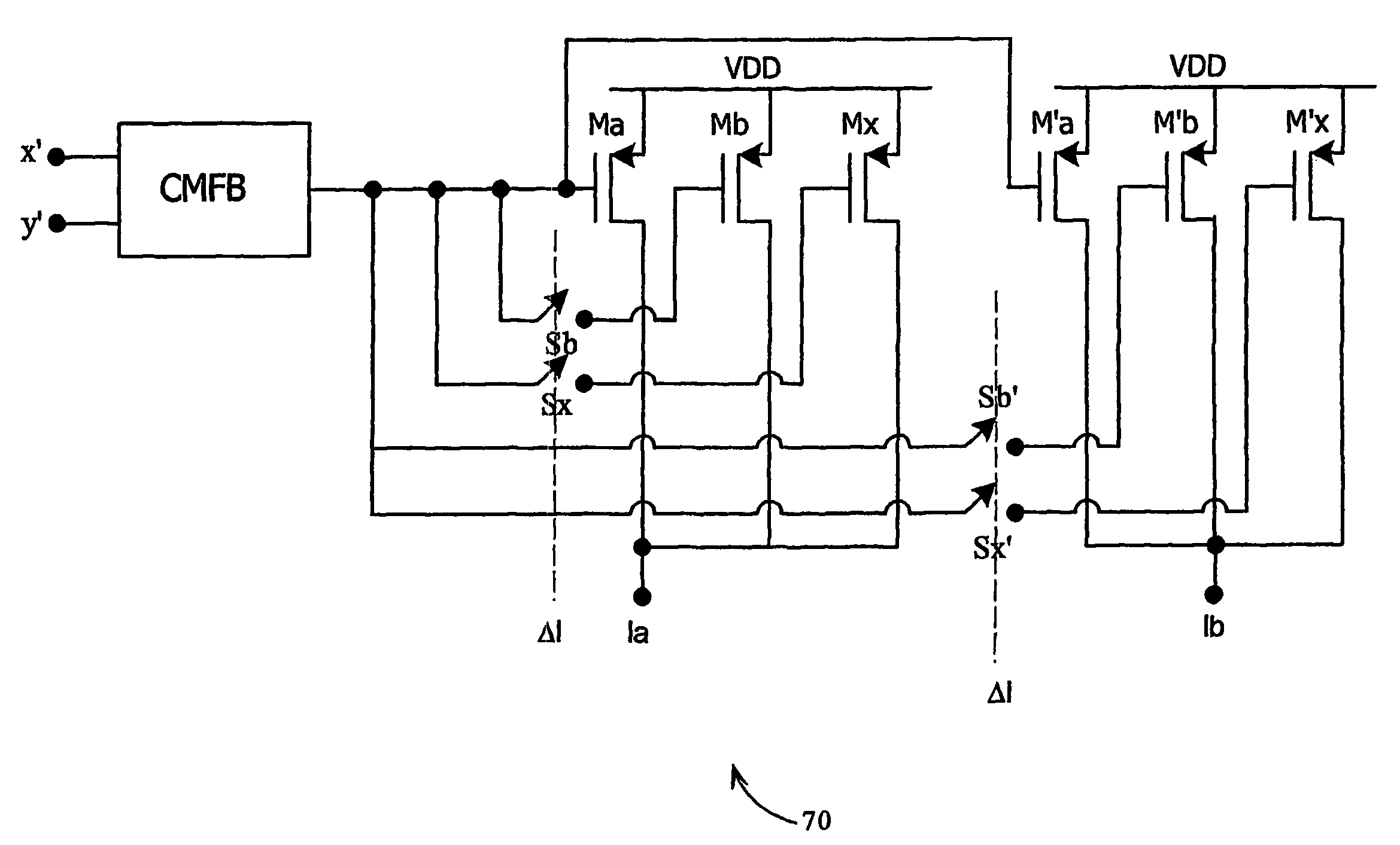
The present invention relates generally to communications, and more specifically to a method and apparatus for minimizing DC offset and second-order modulation products (IM2 noise) while demodulating RF signals. The principle of the invention can be applied to differential, down-conversion circuits (50) consisting of two differential mixers (54, 56) in series, a follows: a pair of current sources Ia and Ib are used to provide current to positive and negative channels of the first differential mixer (54). Providing current to the amplifying transistors of the first mixer (54) reduces the current drawn through the active mixer switches, reducing the noise generated. The current sources 1a and 1b are trimmed in a complementary manner where 1a=I+Delta1, and 1b=Delta1. The value of Δ1 can be determined in a number of manners; for example, it could be established by testing after the circuit has been fabricated, and the value stored on-chip, for future use.

Description

[0001]The present invention relates generally to communications, and more specifically to a method and apparatus for minimizing DC offset and second-order modulation products (IM2 noise) while demodulating RF (radio frequency) signals. The preferred embodiment of the invention marks a significant advance in satisfying the need for an inexpensive, high-performance, fully-integrable, receiver or transceiver.BACKGROUND OF THE INVENTION[0002]Many communication systems modulate electromagnetic signals from baseband to higher frequencies for transmission, and subsequently demodulate those high frequencies back to their original frequency band at the receiver. The original (or baseband) signal may contain, for example: data, voice or video content These baseband signals may be produced by transducers such as microphones or video cameras, be computer generated, or be transferred from an electronic storage device. In general, the use of high frequencies provides longer range and higher capac...

Claims


Application Information

Patent Timeline
Patent Type & Authority Patents(United States)
IPC IPC(8): H04B1/26H03D7/14H03D7/16H04L25/06H04L25/08
CPCH03D7/1441H03D7/161H04B1/26H04L25/061H04L25/085H03D7/1433H03D7/1458H03D7/1466H03D2200/0043H03D2200/0047H03D2200/0084H03D2200/009
Inventor MANKU, TAJINDER
Owner ICERA CANADA ULC
Learn More