ROM embedded DRAM with anti-fuse programming

a technology of anti-fuse programming and embedded dram, which is applied in the field of memory devices, can solve the problems of increasing the overall cost of device fabrication, high cost and feasibility, and relatively low impedance of the dielectric layer

Inactive Publication Date: 2007-05-15
MICRON TECH INC
View PDF8 Cites 10 Cited by
  • Summary
  • Abstract
  • Description
  • Claims
  • Application Information

AI Technical Summary

Benefits of technology

[0017]In another embodiment, a method of providing a read only memory (ROM) embedded dynamic random access memory (DRAM) comprises fabricating a ROM array comprising memory capacitor cells, and applying a program voltage to a first plurality of the memory capacitor cells to

Problems solved by technology

The ROM cells and additional circuitry require additional semiconductor wafer space and fabrication process steps that increase the overall costs of device fabrication.
This requires a special mask used during fabrication of the integrated circuit, which is expensive and feasible only when a large quantity of the same data array is required.
To program the anti-fuse, a programming voltage of a sufficient magnitude is applied across the conductive plates causing a “breakdown” of the dielectric layer, which results in the dielectric layer having relatively low impedance.

Method used


Image

  • ROM embedded DRAM with anti-fuse programming
  • ROM embedded DRAM with anti-fuse programming
  • ROM embedded DRAM with anti-fuse programming

Examples


Embodiment Construction

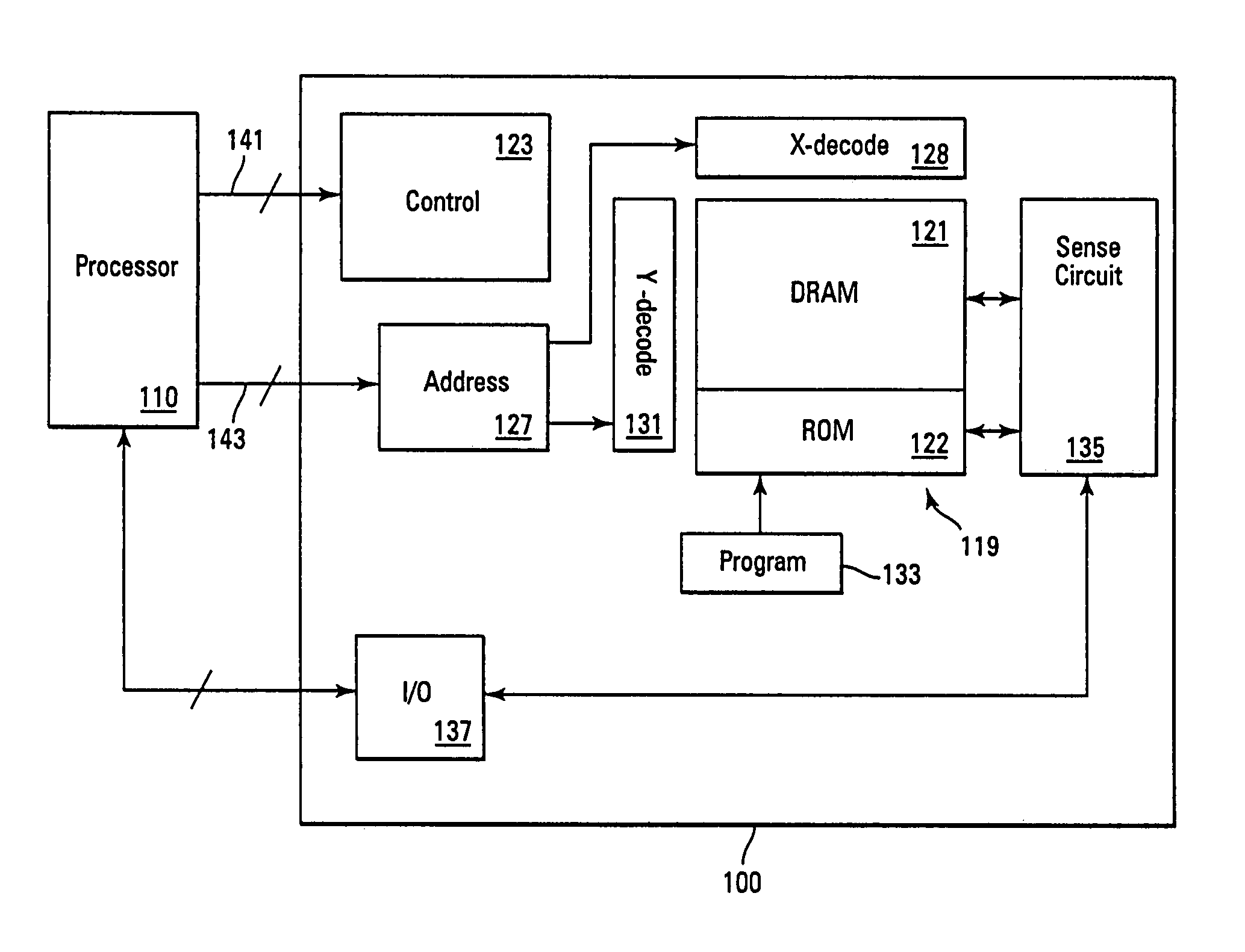
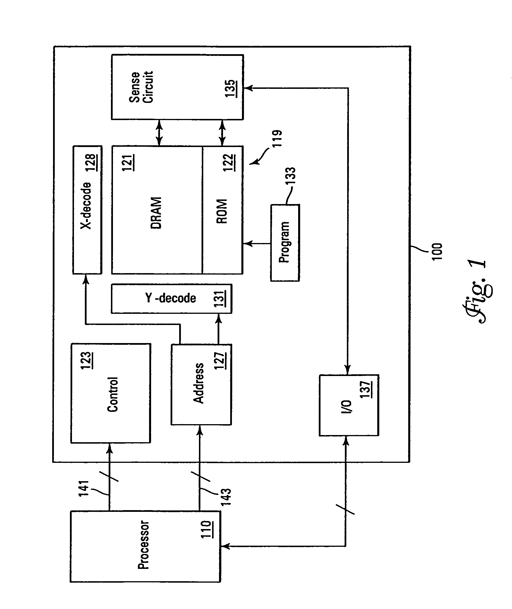
[0027]Referring to FIG. 1, a simplified block diagram of a ROM embedded DRAM 100 of the present invention is described. The memory device can be coupled to a processor 110 for bi-directional data communication. The memory includes an array of memory cells 119. The array includes a dynamic (DRAM) portion 121 and a read only (ROM) portion 122. The ROM array is “embedded” in the dynamic memory and may include some dynamic cells. Control circuitry 123 is provided to manage data storage and retrieval from the array in response to control signals 141 from the processor. Address circuitry 127, X-decoder 128 and Y-decoder 131 analyze address signals 143 and storage access locations of the array. Sense circuitry 135 is used to read data from the array and couple output data to I / O circuitry 137. The I / O circuitry operates in a bi-directional manner to receive data from processor 110 and pass this data to array 119. It is noted that the sense circuitry may not be used in some embodiments to s...


PUM


Abstract

A ROM embedded DRAM provides ROM cells that can be electrically programmed to a data state using DRAM capacitor memory cells. Numerous techniques for reading the memory cells are provided if a single state memory is desired. For example, bias techniques allow un-programmed ROM cells to be read accurately. In one embodiment, the memory includes program circuitry to short capacitor plates together by breaking down an intermediate dielectric layer using anti-fuse programming techniques.

Description

RELATED APPLICATION[0001]This Application is a Continuation of U.S. application Ser. No. 10 / 190,631 filed Jul. 8, 2002 now U.S. Pat. No. 6,735,108, which is incorporated herein by reference.TECHNICAL FIELD OF THE INVENTION[0002]The present invention relates generally to memory devices and in particular the present invention relates to read only memory (ROM) embedded in a dynamic random access memory (DRAM).BACKGROUND OF THE INVENTION[0003]Semiconductor memory systems are comprised of two basic elements: memory storage areas and memory control areas. DRAM, for example, includes a memory cell array, which stores information, and peripheral circuitry, which controls the operation of the memory cell array.[0004]DRAM arrays are manufactured by replicating millions of identical circuit elements, known as DRAM cells, on a single semiconductor wafer. A DRAM cell is an addressable location that can store one bit (binary digit) of data. In its most common form, a DRAM cell consists of two cir...

Claims


Application Information

Patent Timeline
IPC IPC(8): G11C11/24G11C17/16G11C17/18
CPCG11C17/18G11C17/16
Inventor KURTH, CASEYDERNER, SCOTTWALD, PHILLIP G.
Owner MICRON TECH INC
Why Eureka
Try Eureka