
Semiconductor device and semiconductor integrated circuit device

a semiconductor integrated circuit and semiconductor technology, applied in the direction of semiconductor devices, electrical devices, transistors, etc., can solve the problems of insufficient constitution in view of latch-up resistance, soft-error resistance, and information accumulated in the diffusion layer of the node, etc., to achieve the effect of improving the soft-error resistance and the latch-up resistance, and improving the latch-up resistan

Inactive Publication Date: 2007-05-08
RENESAS ELECTRONICS CORP
View PDF11 Cites 14 Cited by
  • Summary
  • Abstract
  • Description
  • Claims
  • Application Information

AI Technical Summary

Benefits of technology

This configuration achieves a better balance between soft-error and latch-up resistance by increasing the resistance of the first region and reducing electron collection, thereby improving the overall performance of the semiconductor device.

Problems solved by technology

In modern large scale semiconductor integrated circuit devices (hereinafter referred to as “LSIs”), a scale reduction of node diffusion layers of memory cells is achieved by miniaturization and / or reducing operating voltage, and the resistance to the soft-error problem, in which the information accumulated in the node diffusion layer is typically inverted, becomes a problem.
It is known that electron-positive hole pairs are generated in the substrate by alpha particles or cosmic ray-origin neutrons generated from a package or a wiring material of a LSI, and a few carriers flow into the node diffusion layer to change the electric potential of the diffusion layer, thereby causing the soft-error.
Further, since secondary ion generated by a nuclear reaction (nuclear crushing reaction) of neutron and silicon helps generating about 10-folds electron-positive hole pairs in comparison with the case of alpha particles, the soft error, which may induce the electric potential inversion of the general logic circuit in addition to memory cell, may be caused.
Although the latch-up resistance in the conventional technology caused by the source voltage-originated trigger (trigger of the break-down of the PN junction or the break-down between SDs of a MOSFET) is gradually improved by lowering the operating voltage of the LSI in recent years, there is still a room for further improving other problems such as external noise and the like.
However, since such configuration provides electric connections for the P wells 202 by disposing P well electric potential junction 204 in every several memory cells (every bit), effective resistances of the P wells 202 is increased, and thus it is subjected to provide insufficient constitution in view of the latch-up resistance.
Therefore, such configuration reduces the effective resistance of the P well, and thus is effective in improving with latch-up resistance.
However, the improvement may be difficult in the structure such as memory cell, in which the MOSFETs are packed therein in the example of the disclosed technology, due to the transverse diffusion caused during the high-energy ion implantation.
However, it is difficult to adopt the SOI substrate to the commercial production, because of the higher price of the SOI substrate, the difficulty in decreasing the size of the memory cell due to the necessity for the body contact in order to inhibit the operation of the parasitic bipolar device, the problems on the manufacturing process specified to the SOI substrate (e.g., silicidation is difficult) or the like.
It has now been discovered that, in the conventional LSI, when the impurity-containing layer is formed on the layer underlying the well to completely isolate the well from the substrate, resulting in improving the soft-error resistance, the trade-off is that the latch-up countermeasure easily becomes to be insufficient, since the manner of drawing the well electric potential / substrate electric potential is not optimum.
On the other hand, when the well is partially in contact with the substrate to improve the latch-up resistance, insufficient countermeasures for the soft-error is provided since insufficient isolation of the well is provided.

Method used


Image

  • Semiconductor device and semiconductor integrated circuit device
  • Semiconductor device and semiconductor integrated circuit device
  • Semiconductor device and semiconductor integrated circuit device

Examples


first embodiment

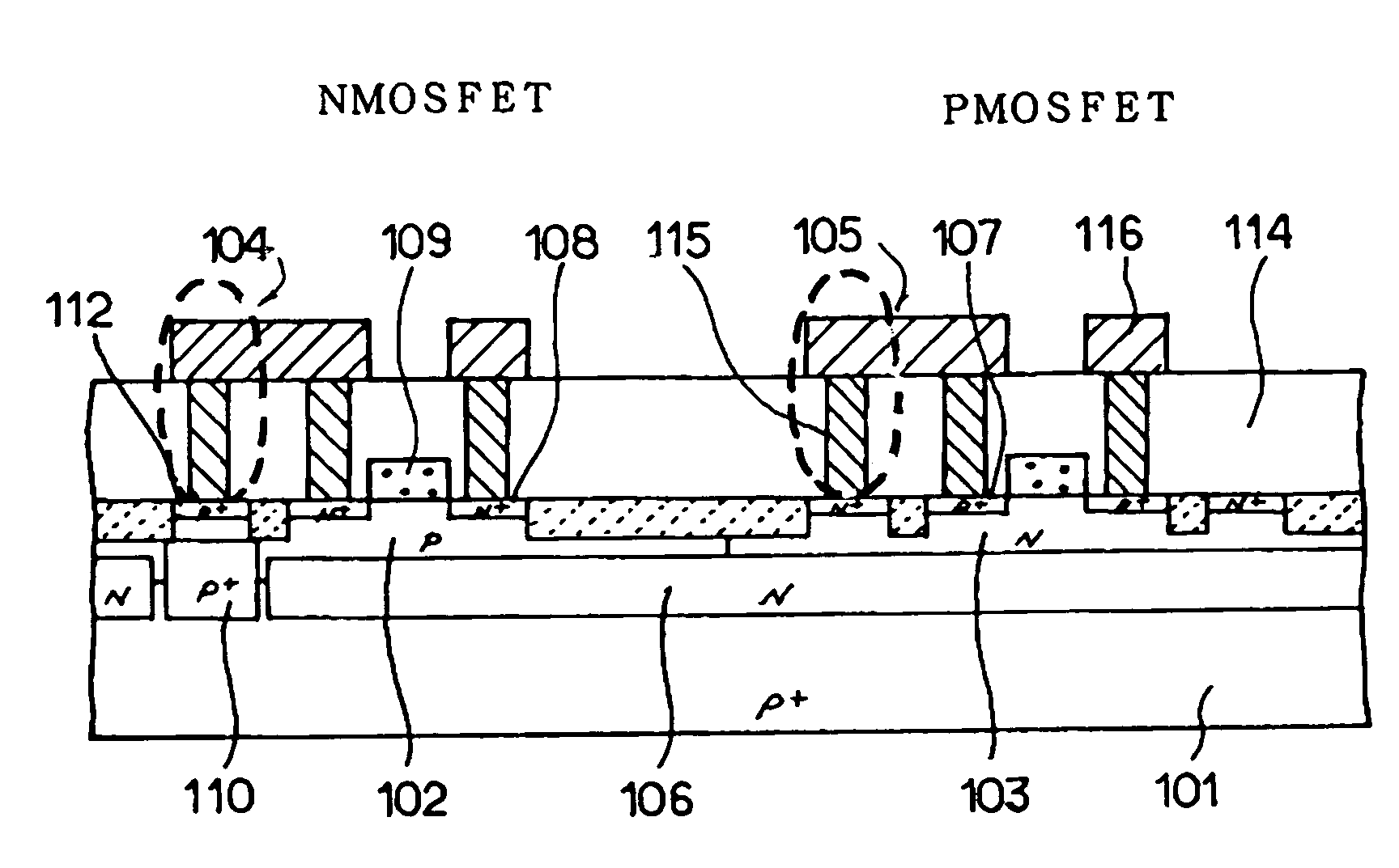
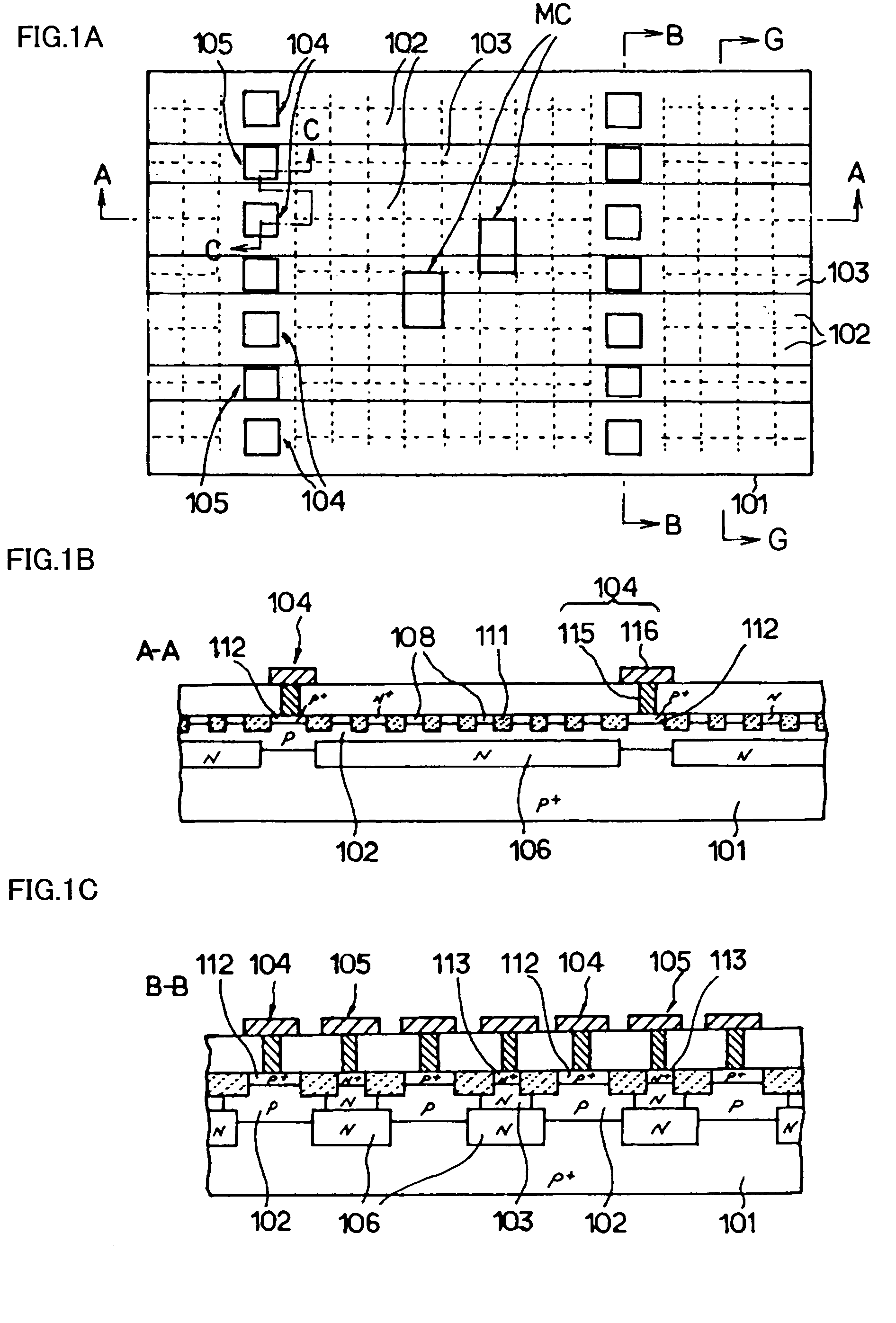
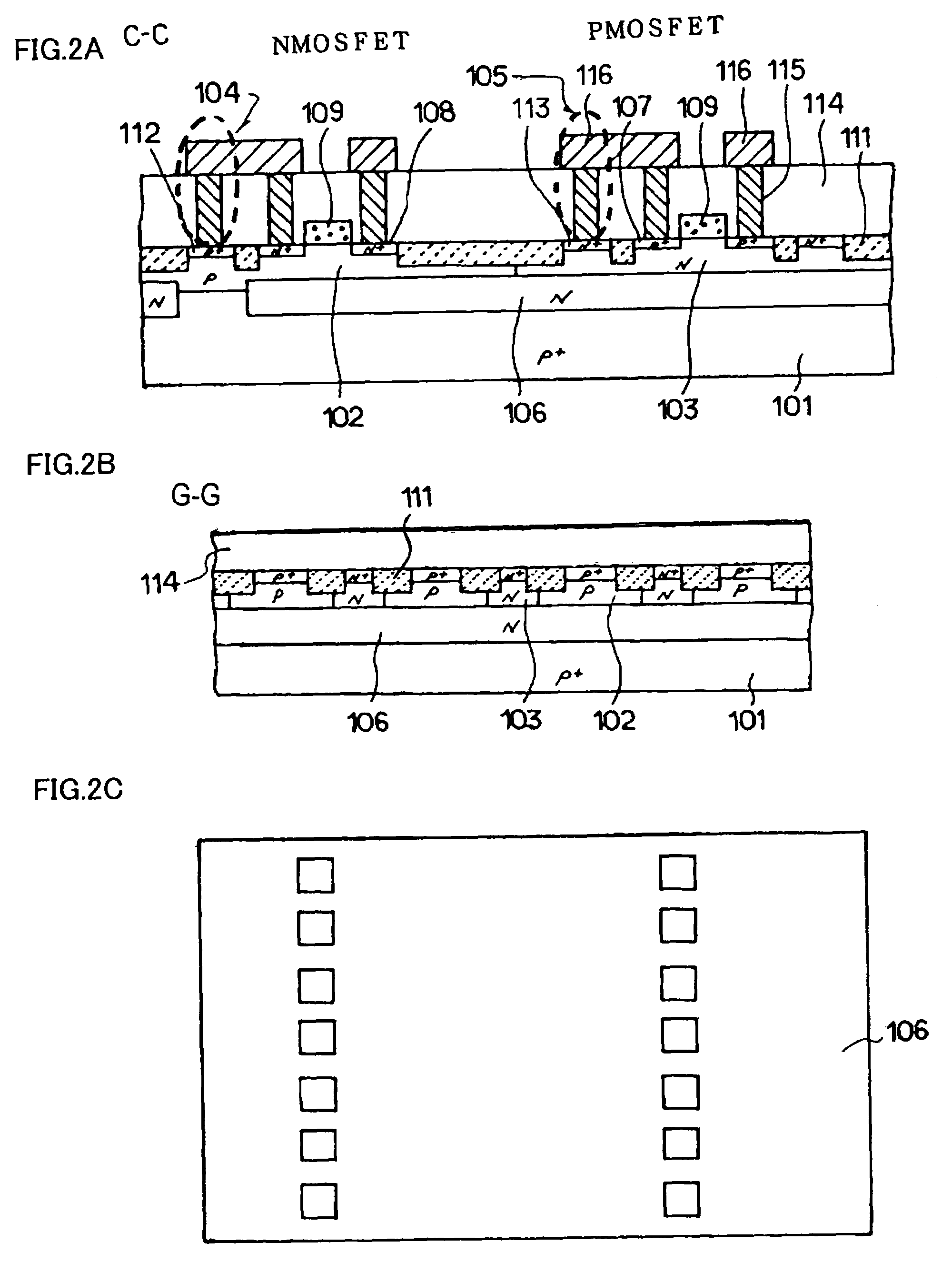
[0030]Embodiments of the present invention will be described as follows, in reference with the annexed figures. FIG. 1A is a schematic plan view of a cell array comprising a plurality of CMOS type SRAM cells. FIG. 1B and FIG. 1C are cross-sectional views cut along line A—A and line B—B of FIG. 1A, respectively. In FIG. 1A, a CMOS type SRAM cell portion includes a NMOSFET (N-channel type MOS field effect transistor), which is not shown and disposed in a region of a P well 102, and a PMOSFET (P-channel type MOS field effect transistor), which is not also shown and disposed in a region of a N well 103, and the PMOSFET and the NMOSFET are electrically coupled to form a memory cell “MC”. Here, since the configuration of the memory cell itself is identical to that having the circuit structure conventionally provided, the detailed description thereof is omitted. The aforementioned P wells 102 and N wells 103 are alternately disposed in a band-like manner to form one (1 bit) memory cell “MC...

second embodiment

[0043]The present invention is not only applicable to the memory cells as illustrated in first embodiment, but can also be applicable to peripheral circuits of LSI (usual CMOS logic circuits). FIG. 7A is a plan view of the main part of the structure illustrated in second embodiment, in which the present invention is applied to the peripheral circuits, and FIG. 7B is a cross-sectional view of the structure shown in FIG. 7A along line D—D, and the same numeral number is assigned to the equivalent element appeared in first embodiment. NMOSFET and PMOSFET are formed in the P well 102 and the N well 103 formed in the P on P+ substrate 101, respectively. In addition, a buried N well 106 is provided in layer under the aforementioned P well 102 and N well 103 in the aforementioned P on P+ substrate 101. In addition, the P well electric potential junction 104 for providing the substrate electric potential of the NMOSFET, or in other words the predetermined electric potential of the P well 10...


PUM


Abstract

Soft-error resistance and latch up resistance are simultaneously improved for LSI involving miniaturization and reducing operating voltage. P wells and N wells are formed in a higher density substrate (P on P+ substrate), and buried N wells are formed on a layer underlying thereof. A PMOSFET is formed in the N well and a NMOSFET is formed in the P well. A P well electric potential junction for coupling P well electric potential of the P well to predetermined electric potential is provided, and a region directly under the P well electric potential junction is provided with a region where the aforementioned buried N well is not disposed. The soft-error resistance is improved by having the buried N well therein, and the latch up resistance is improved by coupling the P well to the substrate.

Description

[0001]This application is based on Japanese patent application NO.2003-376664, the content of which is incorporated herein by reference.BACKGROUND OF THE INVENTION[0002]1. Field of the Invention[0003]The present invention relates to a semiconductor device and a semiconductor integrated circuit device.[0004]2. Related Art[0005]In modern large scale semiconductor integrated circuit devices (hereinafter referred to as “LSIs”), a scale reduction of node diffusion layers of memory cells is achieved by miniaturization and / or reducing operating voltage, and the resistance to the soft-error problem, in which the information accumulated in the node diffusion layer is typically inverted, becomes a problem. It is known that electron-positive hole pairs are generated in the substrate by alpha particles or cosmic ray-origin neutrons generated from a package or a wiring material of a LSI, and a few carriers flow into the node diffusion layer to change the electric potential of the diffusion layer...

Claims


Application Information

Patent Timeline
Patent Type & Authority Patents(United States)
IPC IPC(8): H01L29/94H01L27/04H01L21/822H01L21/8238H01L27/08H01L27/092H01L27/10H01L29/76H10B10/00H10B99/00
CPCH01L27/105H01L27/11H01L27/1052H01L27/0921H10B10/00
Inventor USHIRODA, MASARUFURUTA, HIROSHI
Owner RENESAS ELECTRONICS CORP
Learn More