Semiconductor device
a technology of semiconductor devices and semiconductors, applied in the direction of semiconductor devices, electrical equipment, transistors, etc., can solve the problems of reducing the width of the gate electrode to about 0.1 m, the ion implantation cannot be completed within an actual processing time, and it is difficult to maintain an insulating state between adjacent transistors, so as to reduce the size and prevent the effect of punching
- Summary
- Abstract
- Description
- Claims
- Application Information
AI Technical Summary
Benefits of technology
Problems solved by technology
Method used
Image
Examples
first embodiment
[0047]The first embodiment will be explained.
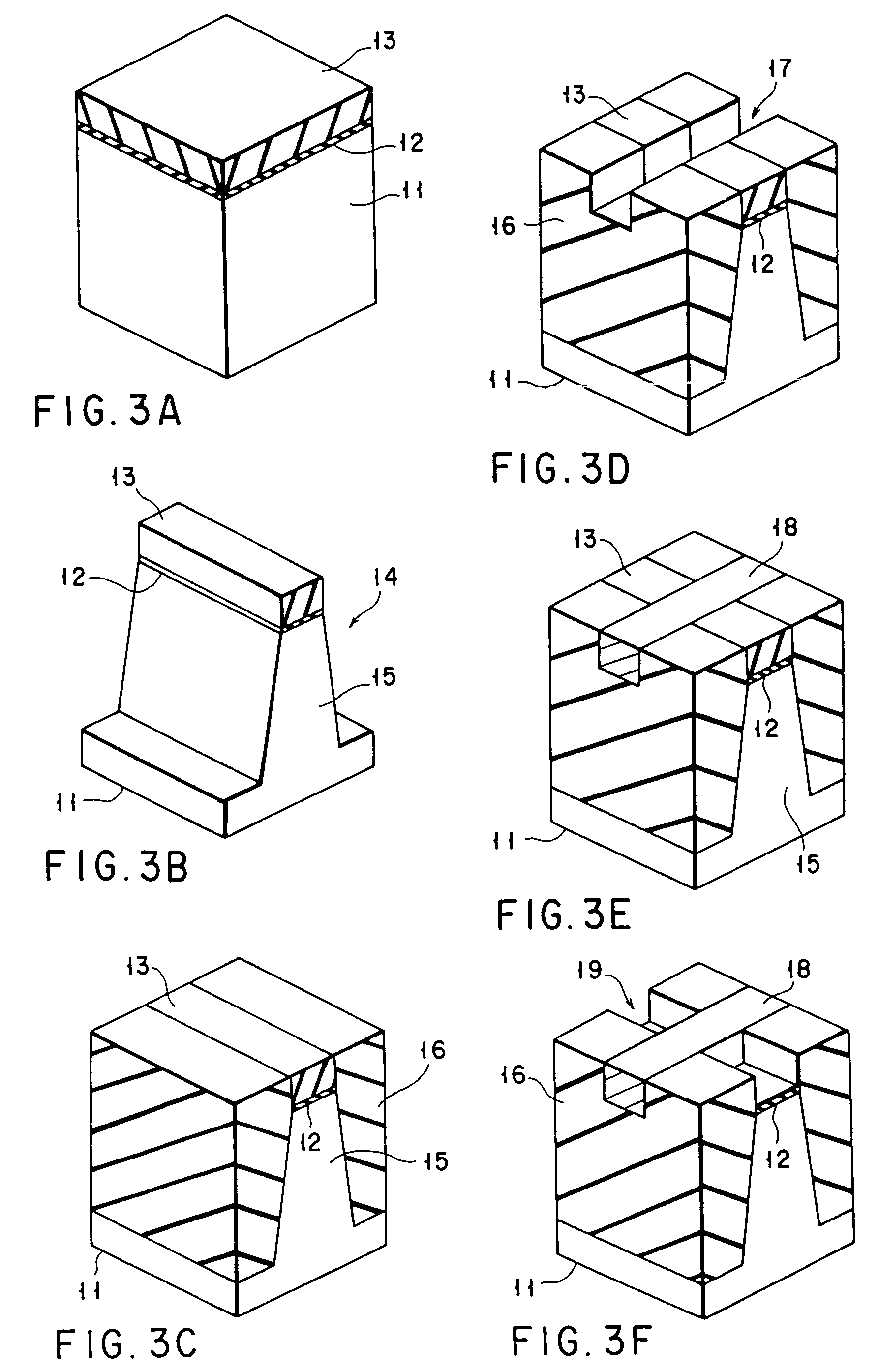
[0048]FIGS. 3A to 3K are perspective views, respectively, schematically showing the manufacturing steps according to the first embodiment of the present invention. The first embodiment will be described with reference to FIGS. 3A to 3K.
[0049]As shown in FIG. 3A, a thermal oxide film 12 having a thickness of about 5 nm is formed on an exposed (100) face of a silicon substrate 11. Silicon nitride is deposited by LPCVD on the thermal oxide film 12 to form a silicon nitride film 13 having a thickness of about 150 nm.
[0050]A resist pattern (not shown) is formed on the silicon nitride film 13 by photolithography or EB lithography. As shown in FIG. 3B, the silicon nitride film 13, the oxide film 12, and the silicon substrate 11 are etched by RIE (Reactive Ion Etching) to form a device region 15. A groove 14 formed at this time is used for device isolation (STI: Sallow Trench Isolation). The trench depth is set to about 300 nm.
[0051]Then, the gro...
second embodiment
[0069]the present invention will be described.
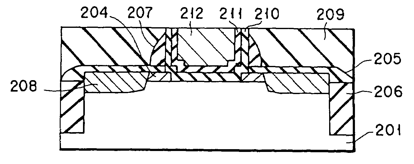
[0070]FIGS. 7A to 7D are sectional views, respectively, schematically showing the manufacturing steps according to the second embodiment of the present invention. Note that the steps in the second embodiment are the same as those in the first embodiment except for only the step shown in FIG. 3I. Only a step corresponding to the step shown in FIG. 3I is therefore explained.
[0071]In the second embodiment, as shown in FIG. 7A, a silicide film 22 does not completely fill a groove in the source / drain region. For this reason, the groove formed by the silicide film 22 is filled with a TEOS oxide film 41 by CVD, and its surface is flattened by CMP, as shown in FIG. 7B. If necessary, the silicide film 22 is recessed by about 50 nm after the step in FIG. 7B, as shown in FIG. 7C. The formed groove is filled with a TEOS oxide film 42 by CVD and flattened, as shown in FIG. 7D. Accordingly, cap films made of the TEOS oxide films 41 and 42 can be forme...
third embodiment
[0073]the present invention will be described.
[0074]FIGS. 8A to 8F are perspective views, respectively, schematically showing the manufacturing steps according to the third embodiment of the present invention. Note that the steps in the third embodiment are the same as the steps shown in FIGS. 3A to 3D in the first embodiment, and subsequent steps are different from the steps in the first embodiment. Therefore, steps subsequent to the step shown in FIG. 3D will be explained.
[0075]As shown in FIG. 8A, an oxide film 12 is removed with an HF-based solution from the bottom of a groove 17 for burying a gate wiring layer. As shown in FIG. 8B, a gate insulating film 51 is formed. Thereafter, a polysilicon film 52 serving as a gate electrode (gate wiring layer) is formed to a thickness of about 300 nm by LPCVD to fill the groove 17, and is flattened by CMP. The surface levels of the polysilicon film 52, a TEOS oxide film 16, and a silicon nitride film 13 are aligned with each other to reali...
PUM
 Abstract
Description
Claims
Application Information
 - R&D
- Intellectual Property
- Life Sciences
- Materials
- Tech Scout
- Unparalleled Data Quality
- Higher Quality Content
- 60% Fewer Hallucinations
Browse by: Latest US Patents, China's latest patents, Technical Efficacy Thesaurus, Application Domain, Technology Topic, Popular Technical Reports.
© 2025 PatSnap. All rights reserved.Legal|Privacy policy|Modern Slavery Act Transparency Statement|Sitemap|About US| Contact US: help@patsnap.com


