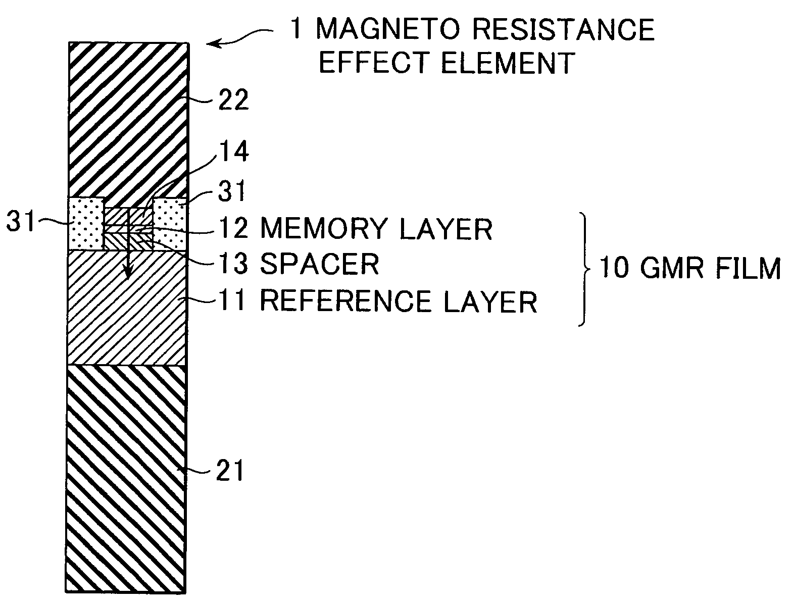
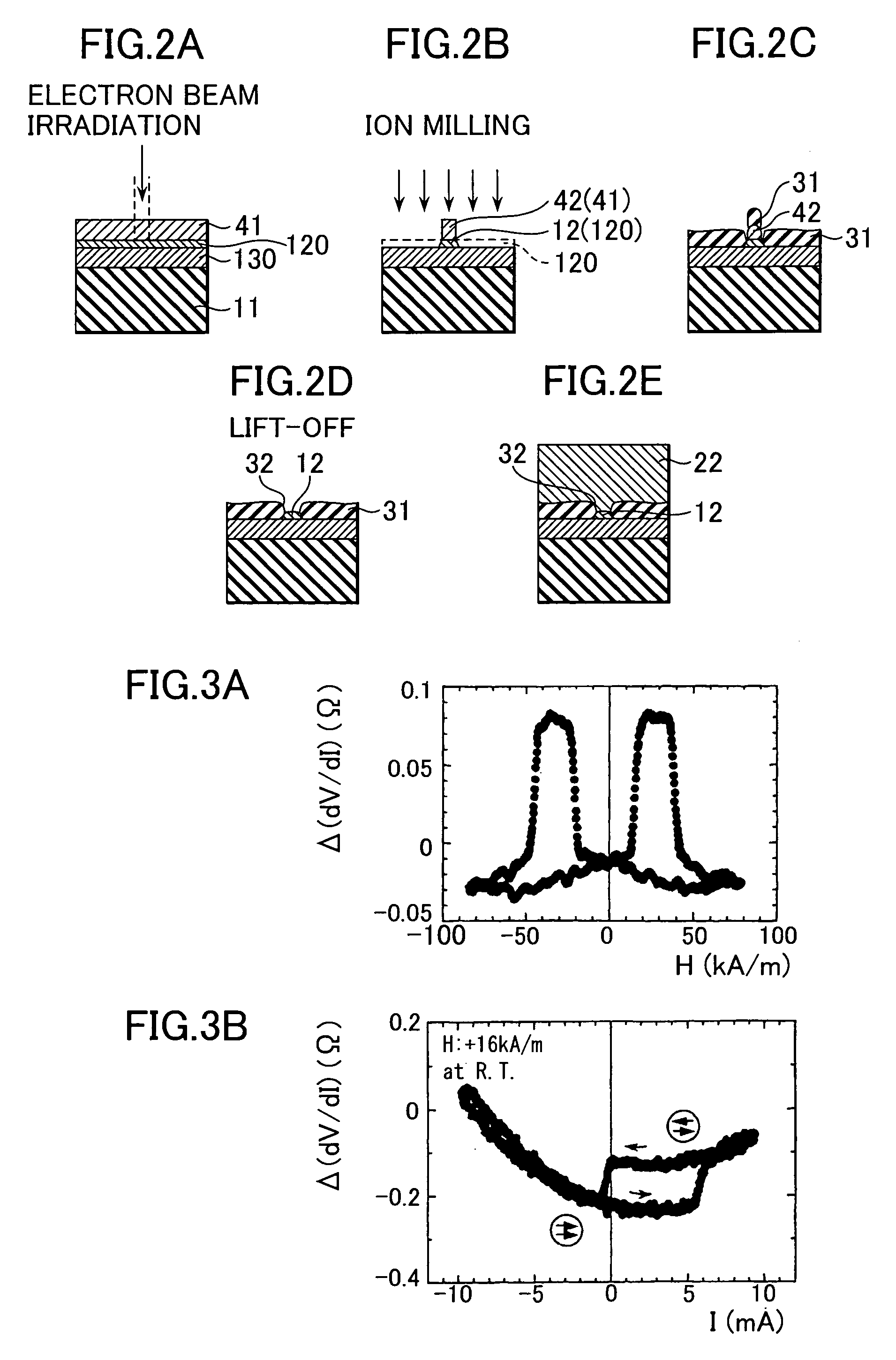
Magnetoresistance effect element, method of manufacture thereof, magnetic storage and method of manufacture thereof
a technology of magnetoresistance and effect elements, which is applied in the field of magnetoresistance effect elements and magnetic storage, can solve the problems of inability to reduce resistance, inhibit any further writing, and increase the required current abruptly,
- Summary
- Abstract
- Description
- Claims
- Application Information
AI Technical Summary
Benefits of technology
Problems solved by technology
Method used
Image

Examples
embodiment
Preferred 4
[0060]A method of manufacturing a magnetic storage according to a preferred embodiment of the present invention will be described in the following.
[0061]With reference to FIG. 6, the method of manufacturing the magnetic storage (e.g. MRAM) according to the preferred embodiment of the present invention is comprised of the steps of: forming a transistor 110 on a semiconductor substrate 101 by a method of forming a conventional field effect transistor, that is, after forming a gate insulation film 111 on the semiconductor substrate 101, a gate electrode 112 is formed thereon; forming a drain region 113 and a source region 114 on both sides of the gate electrode 112 in the semiconductor substrate 101; forming an insulation film 150 to cover the transistor 110; after forming a contact hole which reaches the drain region 113 of the transistor 110 through the insulation film 150, forming an electrode 160 which communicates with the drain region 113 through the contact hole; and...
PUM
| Property | Measurement | Unit |
|---|---|---|
| length | aaaaa | aaaaa |
| length | aaaaa | aaaaa |
| length | aaaaa | aaaaa |
Abstract
Description
Claims
Application Information
 - R&D
- Intellectual Property
- Life Sciences
- Materials
- Tech Scout
- Unparalleled Data Quality
- Higher Quality Content
- 60% Fewer Hallucinations
Browse by: Latest US Patents, China's latest patents, Technical Efficacy Thesaurus, Application Domain, Technology Topic, Popular Technical Reports.
© 2025 PatSnap. All rights reserved.Legal|Privacy policy|Modern Slavery Act Transparency Statement|Sitemap|About US| Contact US: help@patsnap.com