
Integrated circuit package with a balanced-part structure

a technology of integrated circuits and components, applied in the direction of electrical equipment, semiconductor devices, semiconductor/solid-state device details, etc., can solve the problems of small integrated circuit package warpage defects of a substrate warpage defects of the integrated circuit package with only one chip being very small or disappearing, etc., to reduce the warpage degree increase the yield and stability and the effect of the scale of the integrated circuit packag

Inactive Publication Date: 2007-02-13
VIA TECH INC
View PDF10 Cites 112 Cited by
  • Summary
  • Abstract
  • Description
  • Claims
  • Application Information

AI Technical Summary

Benefits of technology

This approach effectively reduces warpage defects, increases the yield and stability of integrated circuit packages, and prevents chip cracking or spalling by balancing mechanical and thermal stress, even in smaller package sizes.

Problems solved by technology

The problems about mechanical stress and thermal mechanical stress of the integrated circuit packages become obviously as more as the integrated circuit packages are smaller.
A little integrated circuit package may get warpage defects of a substrate of the integrated circuit package due to the non-uniform mechanical stress and the non-uniform thermal stress on the substrate while the chips operating.
So that warpage defect of the integrated circuit package with only one chip is usually very small or disappeared because thermal stress inside the integrated circuit package balances very well.
Hence warpage defects of the substrate and the integrated circuit package would appear because of thermal stress caused from operating chips.
Warpage defects affect the operation of the integrated circuit package and spall or crack the chips fastened on the substrate.
Thus, the quality of the integrated circuit package becomes worse because of the unbalanced stress inside the integrated circuit package.

Method used


Image

  • Integrated circuit package with a balanced-part structure
  • Integrated circuit package with a balanced-part structure
  • Integrated circuit package with a balanced-part structure

Examples


Embodiment Construction

[0034]In the present disclosure, the words “a” or “an” are to be taken to include both the singular and the plural. Conversely, any reference to plural items shall, where appropriate, include the singular.

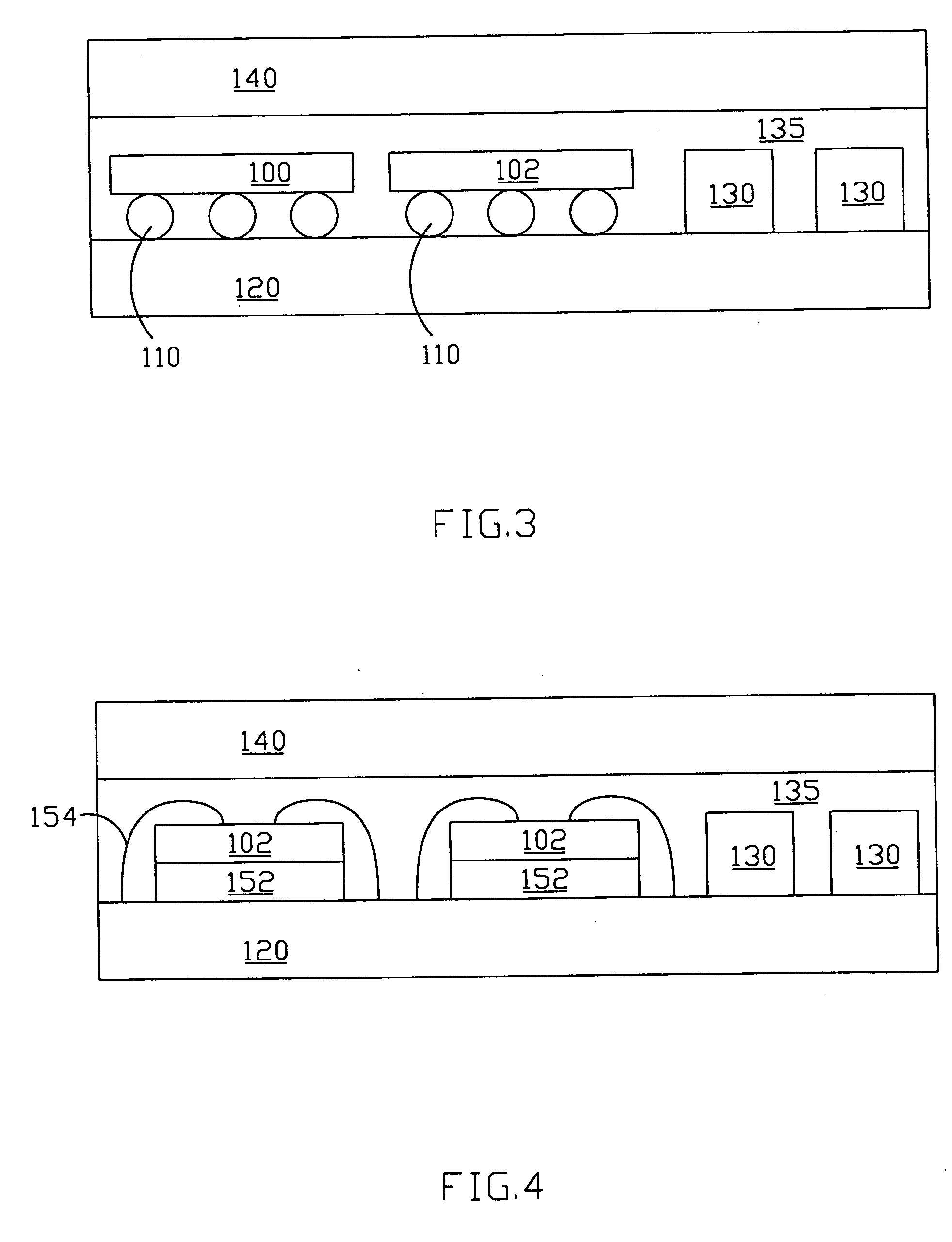
[0035]The preferred embodiment of the present invention provides an integrated circuit package with a balanced-part structure to prevent the integrated circuit package from warpage defects by setting a plurality of the balanced-parts on the substrate of the integrated circuit package. Nonetheless, it should be recognized that the present invention can be practiced in a wide range of other embodiments besides those explicitly described, and the scope of the present invention is expressly not limited except as specified in the accompanying claims.

[0036]As shown in FIG. 1, two chips 100 and 102 are fastened on and connect with a substrate 120 by a plurality of welding parts 110. As shown in FIG. 2, chips 100 and 102 could be fastened on a substrate 120 by bonding layers 150 and 152, r...


PUM


Abstract

An integrated circuit package includes a balanced-part structure. The condition of thermal stress of chips connected on a substrate decides the amount, locations, weights, and the material of at least a balanced-part fastened on a substrate. The balanced-part is fastened on the substrate to balance stress distribution before an adhering heat sinks process and a packaging molding compound process. The balanced-part also decreases thermal stress affection and avoid warpage defects of the integrated circuit packages.

Description

BACKGROUND OF THE INVENTION[0001]1. Field of the Invention[0002]The present invention relates to an integrated circuit package, and more particularly, to an integrated circuit package with a balanced-part structure.[0003]2. Description of the Prior Art[0004]The integrated circuit formed on a semiconductor structure to form an integrated circuit chip is used to be set in a package, i.e. the Quad Flat Package, QFP. The flat package includes leads connected with a lead frame for contacted with the integrated circuit chip. The chip is packaged inside an electric-isolating stable plastic including mechanical support. The leads are soldered on a Printed Circuit Board, PCB.[0005]Many integrated circuit packaging technologies are very important and are improved for packaging the smaller integrated circuit element including million transistor circuits, i.e. the circuits and the dies. The integrated circuit is formed on a silicon wafer through many processes, i.e. the etching process, the imp...

Claims


Application Information

Patent Timeline
Patent Type & Authority Patents(United States)
IPC IPC(8): H01L23/02H01L21/56H01L23/367H01L23/433H01L25/065
CPCH01L23/367H01L23/4334H01L25/0655H01L21/563H01L2924/10253H01L24/48H01L2924/3511H01L2224/16H01L2224/48091H01L2224/48227H01L2224/73253H01L2924/00014H01L2924/00H01L2924/14H01L2924/181H01L2224/73265H01L2924/00012H01L2224/45099H01L2224/45015H01L2924/207
Inventor HO, KWUN YAOKUNG, MORISSKU, TERRYLIAO, ANDY
Owner VIA TECH INC
Learn More