
Dual reactance low noise modular connector insert

a modular connector and low noise technology, applied in the direction of coupling devices, two-part coupling devices, electrical devices, etc., can solve the problems of loss of intended signals, noise in connection with data transmissions, and primary limiting factors of communication systems performan

Inactive Publication Date: 2007-02-06
ORTRONICS INC
View PDF44 Cites 24 Cited by
  • Summary
  • Abstract
  • Description
  • Claims
  • Application Information

AI Technical Summary

Benefits of technology

[0029]The present disclosure provides a modular plug dielectric insert device for a data / voice communication system modular jack housing that advantageously reduces NEXT and FEXT.
[0030]In another aspect of the present disclosure, a modular plug dielectric insert device is disclosed that is particularly adapted for being seated in a data / voice communication system modular jack housing that will reduce signal delay from the plugs input to the IDC terminal outputs to better control NEXT and FEXT of a connecting hardware.
[0031]In addition, a modular jack dielectric insert device for data / voice systems is provided that will not deform the wire pairs in a standard EIA T568B style wire configuration and is simple, low cost and easy to implement into a modular housing. Preferred lead frame wires according to the present disclosure are simple in form, but are precisely bent in proper direction(s) to reduce noise and re-balance the signal pairs in a simple and low cost manner, without reducing the impedance characteristics of the wire pairs.
[0040]The electrical noise may be reduced by the positional relationship which advantageously results in a combination of dual and separate signal feedback reactances. The reactances in the insert device compensate for pair to pair NEXT, FEXT and impedance in a simple and cost effective unit solution.

Problems solved by technology

These distortions and unwanted signals are commonly collectively referred to as “electrical noise,” or simply “noise.” Noise is a primary limiting factor in the performance of a communication system.
Many problems may arise from the existence of noise in connection with data transmissions, such as data errors, system malfunctions and / or loss of the intended signals.
The transmission of data, by itself, generally causes unwanted noise.
Such internally generated noise arises from electromagnetic energy that is induced by the electrical energy in the individual signal-carrying lines within the data transfer media and / or data transfer connecting devices, such electromagnetic energy radiating onto or toward adjacent lines in the same media or device.
Thus, there inherently exists an opportunity for significant crosstalk interference.
NEXT increases the additive noise at the receiver and therefore degrades the signal to noise ratio (SNR).
The non-use of cable shielding (e.g., a foil or braided metallic covering) in fabricating UTP generally increases the effects of outside interference, but also results in reduced cost, size, and installation time of the cable and associated connectors.
Ground loops may give rise to a current that induces interference within the cable, interference against which the shield was intended to protect.
As the speeds have increased, so too has the noise.
Demands for higher frequencies, more bandwidth and improved systems (e.g., Ethernet 1000 Base-T) on UTP cabling, render existing systems and methods unacceptable.
Although crosstalk noise may be reduced, forming lead frames as disclosed in the Vaden '093 patent is a complex process and the return loss and differential impedance in the circuit is disadvantageously increased for all four pairs.
Section two also aligns the lead frames in an uniformed parallel pattern from lead frame bend location to lead frame stagger array output, which minimizes NEXT, but due to the imbalances of the center wire pairs and FEXT noises are disadvantageously increased according to the Stewart '266 design.
The re-bending of lead frames as disclosed by the Berg '770 and Nordx / CDT '503 patents is an expensive process and the crosstalk reductions addressed by these disclosures occur mainly within the second section of their respective designs.

Method used


Image

  • Dual reactance low noise modular connector insert
  • Dual reactance low noise modular connector insert
  • Dual reactance low noise modular connector insert

Examples


Embodiment Construction

)

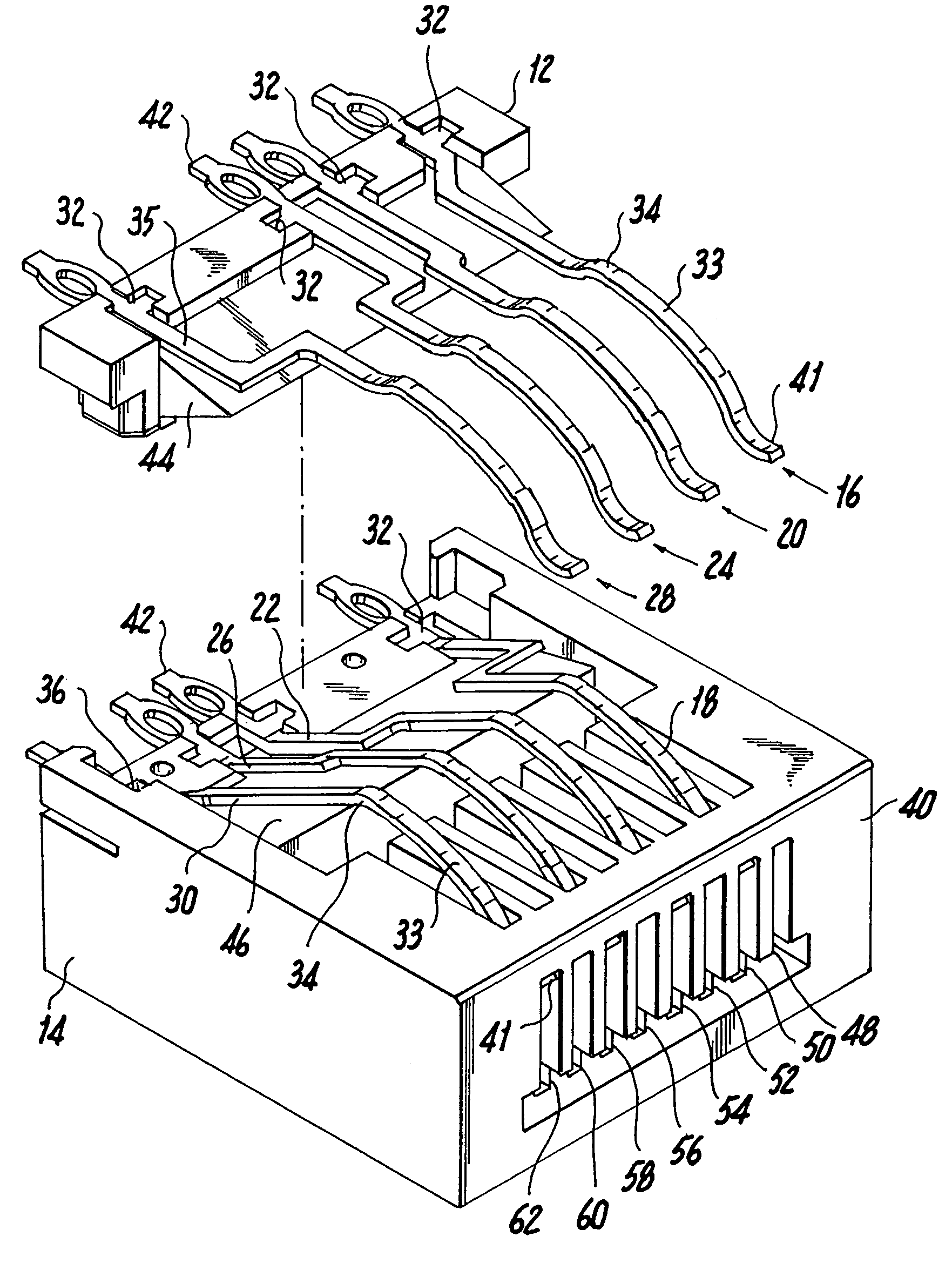
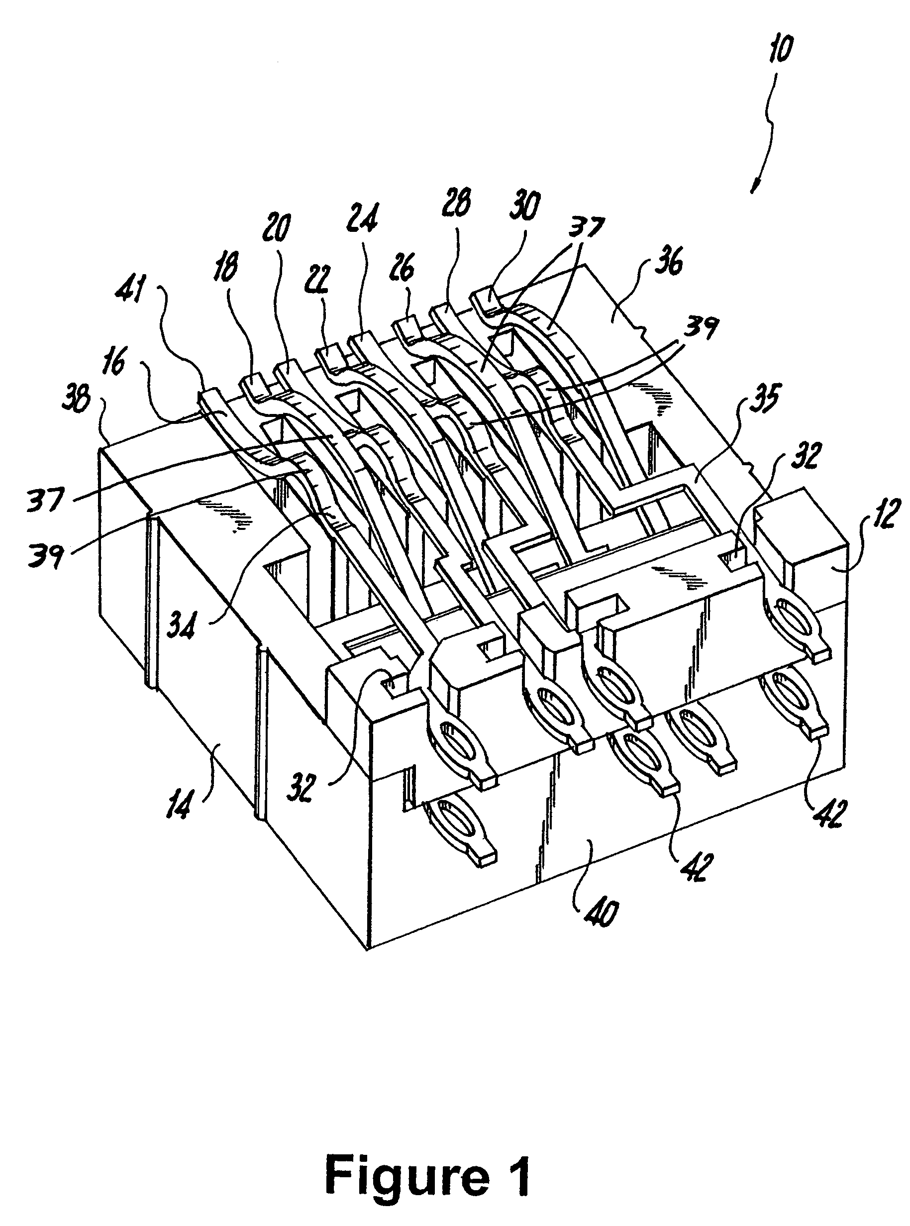
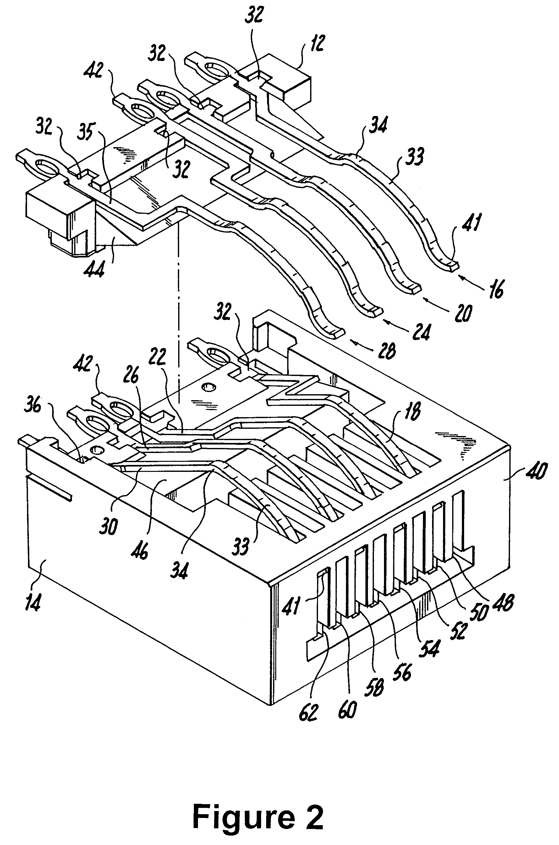
[0057]Referring now to the drawings, FIGS. 1–12 illustrate an embodiment of a dielectric interface modular insert 10 in accordance with the present disclosure. Insert 10 has an upper portion 12 seated on a lower portion 14, with electrically conductive lead frames 16, 18, 20 , 22, 24, 26, 28 and 30 being disposed between. Preferably, upper portion 12 and lower portion 14 are fabricated from a low dielectric material, such as plastic.

[0058]Insert 10 contains terminals having 8 lead frames in accordance with most standard wiring formations, such as the T568B and T568A style RJ45 plugs. The TIA / EIA commercial building standards have defined category 5e and 6 electrical performance parameters for higher bandwidth (100 up to 250 MHz) systems. In category 5e and 6, the TIA / EIA RJ45 wiring style is the preferred formation and is generally followed throughout the cabling industry.

[0059]Lead frames 16 through 30 are engaged in channel slots 32 with cut outs in upper portion 12 and lower por...


PUM


Abstract

The present invention is related to the modular plug housing insert device that makes electrical contact to a telecommunication plug to complete an interface media connection. The positional relationship of the conductors in the modular plug housing insert device are arranged to from capacitance, such that the Near-end Crosstalk (NEXT) and Far End Crosstalk (FEXT) is reduced without compromising impedance.

Description

CROSS-REFERENCE TO RELATED APPLICATION(S)[0001]This application is a continuation application of a entitled “Dual Reactance Low Noise Modular Connector Insert,” which was assigned Ser. No. 09 / 982,073 and which was filed on Oct. 17, 2001 now U.S. Pat. No. 6,896,557. The foregoing non-provisional application claimed the benefit of commonly owned U.S. Provisional Application No. 60 / 282,308, filed Apr. 5, 2001 and entitled “Modular Jack,” the disclosure of which is also herein incorporated by reference.BACKGROUND OF THE DISCLOSURE[0002]1. Technical Field[0003]The present disclosure relates to devices for interfacing with high frequency data transfer media and, more particularly, to modular jack housing inserts, such as those that are used as interface connectors for Unshielded Twisted Pair (“UTP”) media, that advantageously compensate for and reduce electrical noise.[0004]2. Background Art[0005]In data transmission, the signal originally transmitted through the data transfer media is no...

Claims


Application Information

Patent Timeline
Patent Type & Authority Patents(United States)
IPC IPC(8): H01R24/00
CPCH01R13/6474H01R13/6461Y10S439/941H01R24/64
Inventor AEKINS, ROBERT A.KESSLER, GEORGE M.VENDITTI, JAYDUPUIS, JOSEPH E.
Owner ORTRONICS INC
Learn More