
High-speed adaptive interconnect architecture with nonlinear error functions

a nonlinear error, adaptive interconnect technology, applied in the direction of pulse manipulation, pulse technique, digital transmission, etc., can solve the problems of eye closing, inability to discern the transmitted signal level, and eventually the inter-chip communication speed is reduced, and achieves low cost, high speed, and low power equalizing the effect of the receiver structur

Inactive Publication Date: 2007-01-02
RPX CORP
View PDF4 Cites 13 Cited by
  • Summary
  • Abstract
  • Description
  • Claims
  • Application Information

AI Technical Summary

Benefits of technology

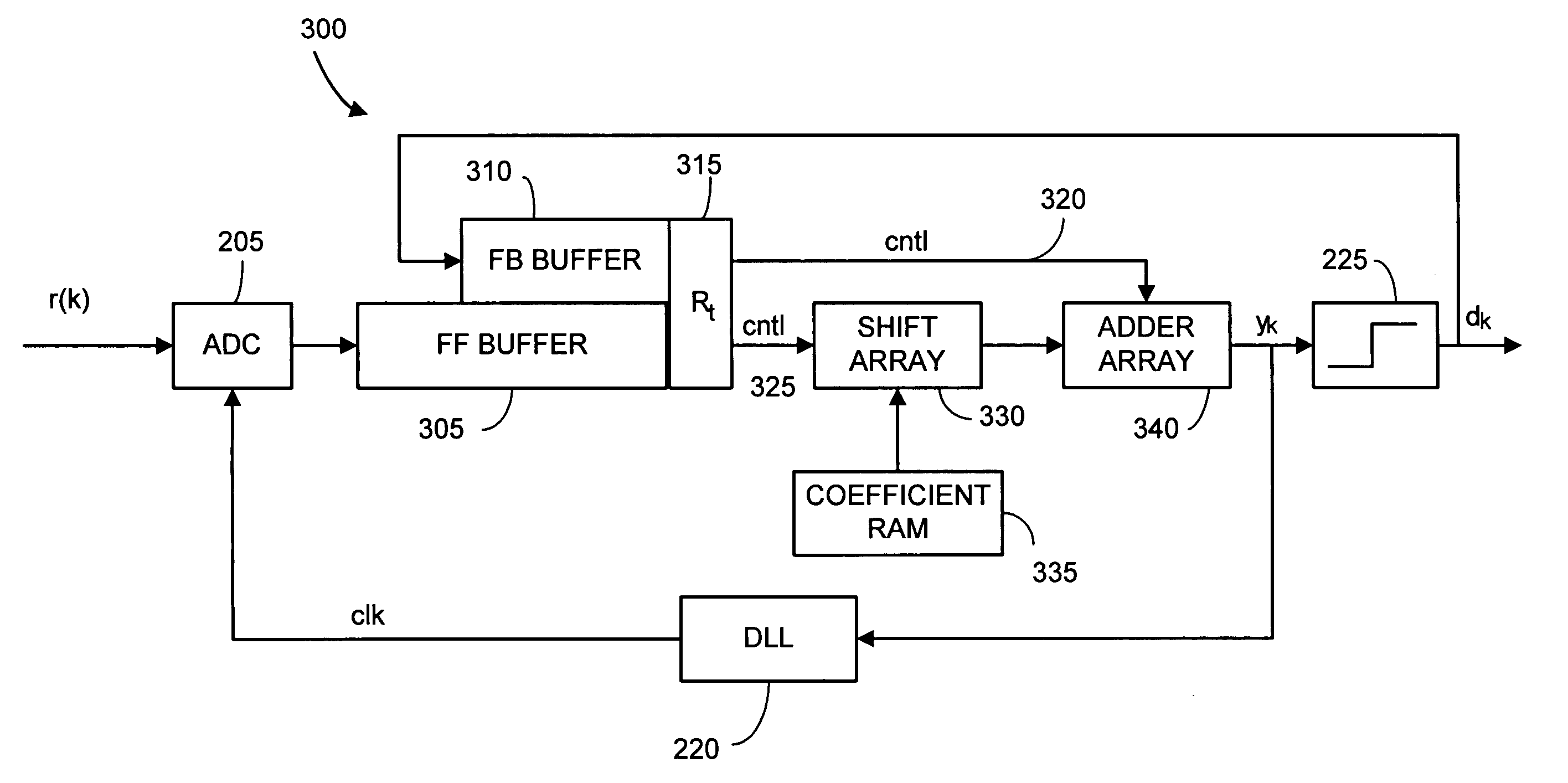
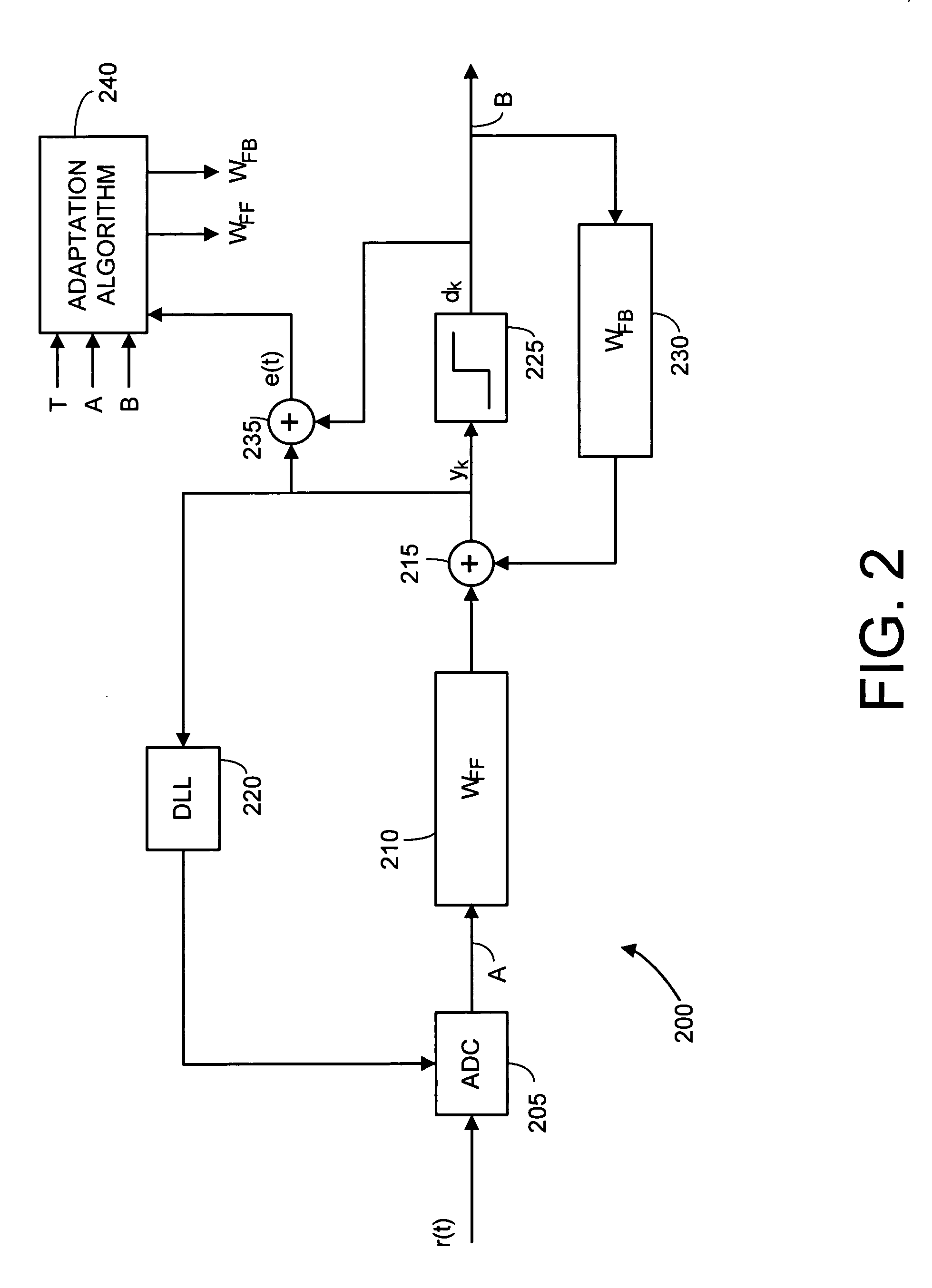
[0009]The present invention overcomes difficulties with prior art inter-chip and inter-module interconnects by introducing a low cost and low power equalizing receiver structure for inter-chip communications. The novel receiver structure allows binary and multilevel signaling to be received at greater speeds and over more diverse paths by processing the received signal prior to signal symbol detection. The equalizer structure can inherently operate at high speeds due to its multiply-free architecture. Both serial and parallel circuit structures are taught. Either of these structures or a hybrid of the two can be selected in light of design constraints. Systems based on symbol-spaced and fractionally-spaced sampling are taught. The equalizer is adaptive, but only needs to be adapted at power-up and can be optionally retuned periodically.

Problems solved by technology

While these multilevel signaling approaches are advantageous, inter-chip communication speeds are eventually limited by a phenomenon known in the art as “inter-symbol interference” or, “eye-closing.” Eye closing occurs when distortions introduced by the communication channel make it impossible to discern the transmitted signal levels by sampling the received waveform.
The problem of eye closing becomes more severe on a given connection as the data rate is increased.
In future wafer scale designs, the same problems may occur for longer runs between intra-wafer modules.
Equalization approaches are multiply-accumulate intensive and rely on DSP (digital signal processing).
Hence prior art solutions are too expensive for inter-chip applications where the symbol rates are presently in the 800 MHz region.
Prior art DSP-based equalizers are not suited to solve such inter-chip equalization problems in a cost efficient way.

Method used


Image

  • High-speed adaptive interconnect architecture with nonlinear error functions
  • High-speed adaptive interconnect architecture with nonlinear error functions
  • High-speed adaptive interconnect architecture with nonlinear error functions

Examples


Embodiment Construction

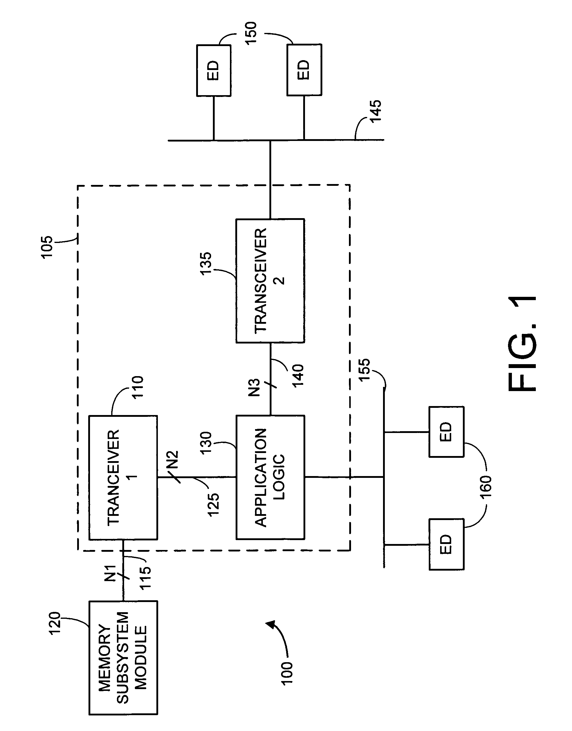
[0018]FIG. 1 is a block diagram illustrating an exemplary electronic system 100 making use of a bus line receiver structure in accordance with the present invention. A processing device 105 is illustrated that may be implemented with various combinations of one or more bus receiver modules (110, 135 and logic coupling to bus 155). These modules may be implemented on one or more single chip dies. In a preferred embodiment the processing device 105 is implemented as a microsystem on a single die. In most preferred embodiments, the bus receiver modules also include transmit (write) capabilities and are technically “transceivers modules.” As this application focuses mainly on the bus receiver aspect, these modules will be discussed as receivers, but at times may also be referred to as “transceivers.” It is to be understood that the bus interconnects usually include both read and write capabilities. In this application it is assumed that the bus receiver is responsible, at least in part,...


PUM


Abstract

A low cost and high speed equalizing receiver structure is provided for improved inter-chip and inter-module communications. The receiver is able to recover data from a corrupted waveform from a signal wire such as one found on data, address or control wires in a microsystem architecture. The receiver can be used with binary as well as m-ary pulse amplitude modulation schemes. The receiver can be used to increase the sustainable data rate between chips or can be used to sustain a given data rate over a poorer quality channel as compared to prior art interconnect technologies. Methods for training and operating the receiver structure are provided. A novel structure called the decision feedback equalizer and cross talk canceller (DFE-CTC) is introduced and methods to compute the coefficients to minimize error in terms of the l2 norm, the l∞ norm, and statistical probability of error functions are also disclosed.

Description

[0001]The present application is a continuation-in-part of U.S. patent application Ser. No. 09 / 624,068, filed Sep. Jul. 24, 2000, now U.S. Pat. No. 6,765,958, entitled “high speed adaptive interconnect architecture.”BACKGROUND OF THE INVENTION[0002]1. Field of the Invention[0003]This invention relates generally to VLSI circuits. More particularly, the invention relates to low cost receiver structures and methods to provide high-speed inter-chip or inter-module communication links. Also, the invention relates to the training and operation of non-linear adaptive structures to equalize and reduce cross-talk on high-speed wire traces and inter-wafer traces between chips or wafer sub-modules.[0004]2. Description of the Related Art[0005]Communication between chips on a circuit board traditionally use very simple binary zero-one logic. A high voltage is sent to represent a binary one, and a zero voltage is sent to represent a binary zero. The receiver maintains clock synchronization with t...

Claims


Application Information

Patent Timeline
Patent Type & Authority Patents(United States)
IPC IPC(8): H03H7/30H04L25/45
CPCH04L25/03057H04L25/45H04L2025/03503
Inventor DOWLING, ERIC MORGAN
Owner RPX CORP
Learn More