
Method of forming wirings for tile-shaped elements, structures of wirings for tile-shaped elements, and electronic equipment

a technology of wiring and tile, applied in the direction of conductive pattern formation, thermoelectric devices, printed circuit non-printed electric components association, etc., can solve the problems of substantial time required for wiring work, substantially large manufacturing cost, so as to reduce the waste of liquid material, excellently formed, and high reliability

Inactive Publication Date: 2006-12-19
SEIKO EPSON CORP
View PDF30 Cites 7 Cited by
  • Summary
  • Abstract
  • Description
  • Claims
  • Application Information

AI Technical Summary

Benefits of technology

The invention provides a method for forming electrical wiring on a tile-shaped element that allows for highly reliable electrical connections at a low cost. The method involves coating a liquid material on a wiring region and forming a conductive film to define the electrical wiring. This method eliminates the need for aerial wiring, reduces manufacturing costs, and reduces short-circuit or breakage of wirings. The invention also provides a method for forming a semiconductor device on a final substrate using a sacrificial layer and a semiconductor element separated from the substrate. The semiconductor element can be tested and selected in advance prior to manufacture of integrated circuits. Overall, the invention provides a way to achieve reliable electrical wiring with a minute wiring pattern for thin film devices.

Problems solved by technology

However, when the electrical wiring is formed by aerial wiring, such as wire bonding, the wiring work requires substantial time.
In particular, minute wiring work is difficult and results in a substantially large manufacturing cost.
When the electrical wiring is formed by using a method, such as vapor deposition of metal thin films or photolithography, a substantially large manufacturing cost is required because masks having desired patterns must be formed.
Furthermore, coping with design changes, such as changes in the wiring positions is expensive.

Method used


Image

  • Method of forming wirings for tile-shaped elements, structures of wirings for tile-shaped elements, and electronic equipment
  • Method of forming wirings for tile-shaped elements, structures of wirings for tile-shaped elements, and electronic equipment
  • Method of forming wirings for tile-shaped elements, structures of wirings for tile-shaped elements, and electronic equipment

Examples


first exemplary embodiment

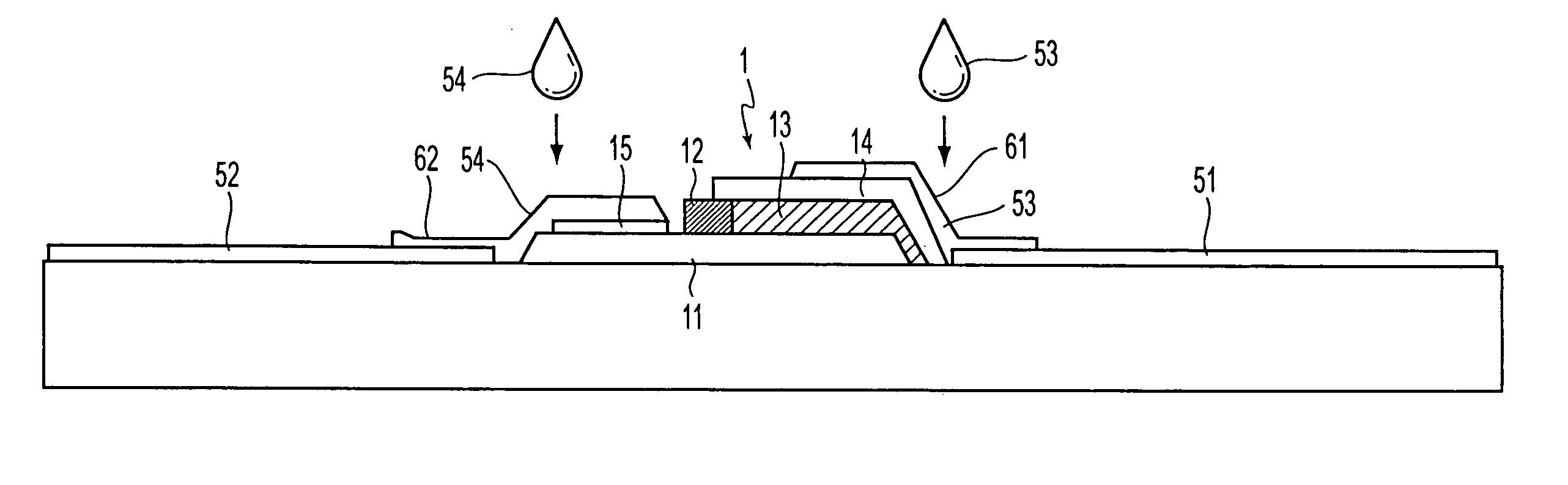
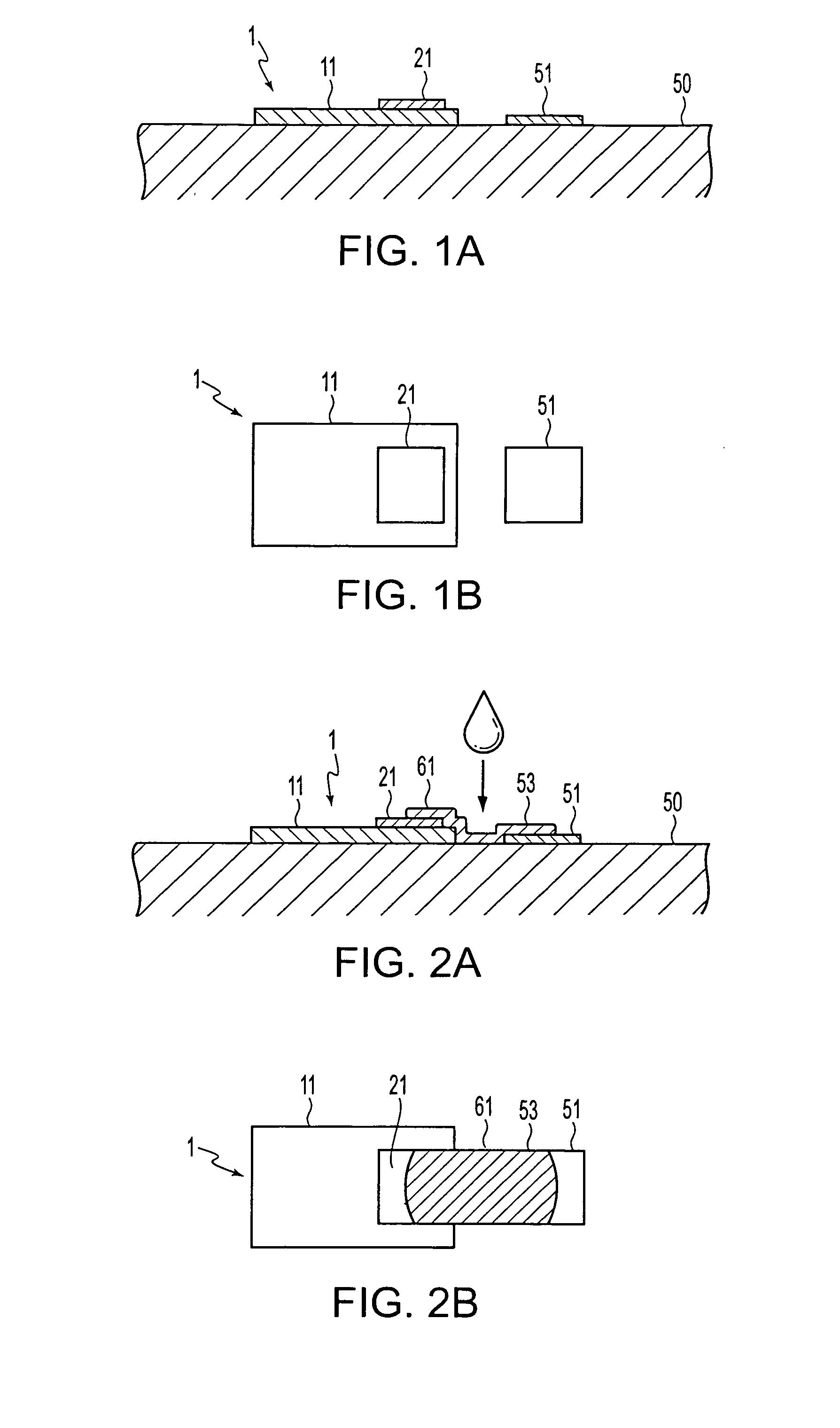
[0040]A wiring forming method for a tile-shaped element and a wiring structure for a tile-shaped element in accordance with a first exemplary embodiment of the invention are described below. As an example of a tile-shaped element in accordance with the present exemplary embodiment, a micro tile-shaped element in a minute tile configuration is described. However, the invention is not limited to this, and can be applied to a tile-shaped element that is not minute. First, a wiring forming method for a tile-shaped element and a wiring structure for a tile-shaped element in accordance with the first exemplary embodiment of the invention are described with reference to FIGS. 1A–B and FIGS. 2A–B.

[0041]FIGS. 1A–B are schematics in which a micro tile-shaped element is bonded to a final substrate. A micro tile-shaped element 1 is equipped with a tile section 11 in a tile configuration and an electrode 21 provided on an upper surface of the tile section 11. The tile section 11 may have a funct...

examples of application

Method

[0050]Next, examples of the method of applying the liquid material 53 to the wiring region 61 are described. For example, a method in which the liquid material 53 is once applied to the entire surface of the final substrate 50 including the surface of the minute tile element 1, and then, the liquid material 53 applied on areas other than the wiring region 61 is removed, to thereby coat the liquid material only on the wiring region 61, can be used. However, according to this method, the amount of the liquid material 53 that becomes wasted is large. Thus, it is desirable to use a method in which the liquid material 53 is initially, selectively applied only to the wiring region 61.

[0051]A droplet discharge method to jet the liquid material 53 as droplets from an ink jet nozzle, that may be used with, for example, an ink-jet printer, or the like, can be used as the method to selectively apply the liquid material 53. Moreover, the liquid material 53 may be discharged as droplets by...

second exemplary embodiment

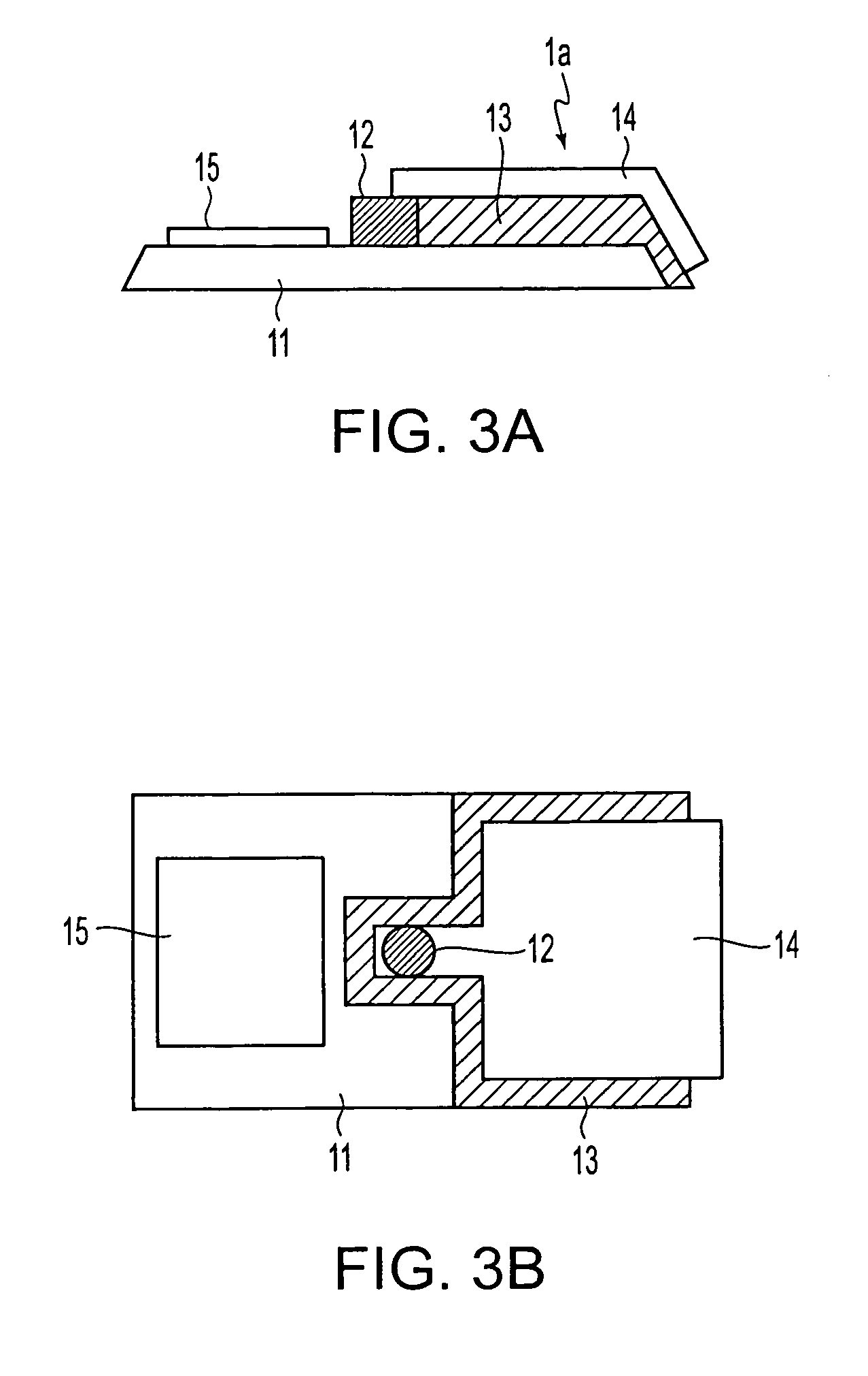
[0055]Next, a wiring forming method for a tile-shaped element and a wiring structure for a tile-shaped element in accordance with a second exemplary embodiment of the invention are described below with reference to FIGS. 3A–B through FIGS. 5A–B. First, a micro tile-shaped element 1a to which the wiring forming method of the present exemplary embodiment is applied is described. FIGS. 3A–B show an example of a micro tile-shaped element in accordance with the second exemplary embodiment. The micro tile-shaped element 1a is a minute semiconductor element in a tile configuration. The micro tile-shaped element 1a is formed from a plate-like member having a thickness of 20 μm or less, and a size in width and length of several ten μm to several hundred μm. In a method for manufacturing the micro tile-shaped element 1a, a sacrificial layer is formed on a semiconductor substrate (first substrate), and a functional layer (electronic functional section) that defines the micro tile-shaped elemen...


PUM


Abstract

Methods are provided to form wirings for tile-shaped elements, structures of wirings for tile-shaped elements, and electronic equipment, with which highly reliable electrical wirings having minute wiring patterns can be formed. In wiring forming method for a tile-shaped element, which is used, when a circuit device is formed by connecting a tile-shaped element having at least an electrode and a tile configuration to a final substrate having at least an electrode, to form an electrical wiring that electrically connects the electrode of the tile-shaped element to the electrode of the final substrate, liquid material including electro conductive material is applied to at least a part of a wiring region that is a region where the electrical wiring is formed on at least one of surfaces of the final substrate and the tile-shaped element.

Description

BACKGROUND OF THE INVENTION[0001]1. Field of Invention[0002]Exemplary aspects of the invention relate to methods of forming wirings for tile-shaped elements, structures of wirings for tile-shaped elements, and electronic equipment.[0003]2. Description of Related Art[0004]The related art includes epitaxial lift-off (ELO) methods, in which semiconductor elements formed on a substrate are diced into micro tile elements (semiconductor elements), each in the shape of a micro tile configuration, and separated from the substrate. The micro tile element is handled and attached to an optional substrate (final substrate), thereby forming a substrate equipped with a thin film device (circuit device). See Japanese Laid-open Patent Application 2000-58562.SUMMARY OF THE INVENTION[0005]In the related art, an electrode (terminal) of the micro tile element is connected with an electrical wiring to an electrode (terminal) of a circuit that is provided on the final substrate. However, for example, whe...

Claims


Application Information

Patent Timeline
Patent Type & Authority Patents(United States)
IPC IPC(8): H01L23/48H01L21/288H05K3/32H01L21/60H05K1/18H05K3/10
CPCB82Y30/00H01L24/24H01L24/82H01L24/83H01L21/288H01L24/29H01L2924/1305H01L33/0079H01L2221/68354H01L2221/68359H01L2221/68368H01L2224/24011H01L2224/24225H01L2224/24226H01L2224/76155H01L2224/83001H01L2224/83192H01L2224/838H01L2224/92244H01L2924/01005H01L2924/01013H01L2924/01015H01L2924/01029H01L2924/01046H01L2924/01047H01L2924/0105H01L2924/01075H01L2924/01078H01L2924/01079H01L2924/01082H01L2924/0781H01L2924/09701H01L2924/10336H01L2924/14H01L2924/19041H01L2924/19042H01L2924/00011H01L2224/82102H01L2924/00013H01L2924/12041H01L2924/0665H01L2924/014H01L2924/01033H01L2924/01006H01L2224/29298H01L2224/2919H01L2924/00H01L2924/3512H01L2224/29099H01L2224/29199H01L2224/29299H01L2224/2929H01L2924/12042H01L2924/12043H01L33/0093
Inventor KONDO, TAKAYUKI
Owner SEIKO EPSON CORP
Learn More