Optical scanning device and image forming apparatus using the same

a scanning device and image forming technology, applied in the direction of inking apparatus, instruments, electrographic processes, etc., can solve the problems of increasing cost, difficult to make the wavelengths completely equal to one another, and limitation of the selection range of wavelengths of light sources, so as to achieve convenient production and improve performance

Inactive Publication Date: 2006-10-24
CANON KK
View PDF12 Cites 7 Cited by
  • Summary
  • Abstract
  • Description
  • Claims
  • Application Information

AI Technical Summary

Benefits of technology

[0022]An object of the present invention is to provide a diffraction grid which can be used for an optical scanning device and easily produced by selecting a suitable design order of the diffraction grid. Another object of the present invention is to provide a diffraction grid that attains a preferable performance even when a short wavelength light source having a wavelength of 500 nm or less is used. Still another object of the present invention is to provide an optical scanning device using the diffraction grid, which has functions such as a chromatic aberration correction and a temperature compensation, and an image forming apparatus using the optical scanning device.

Problems solved by technology

As compared with a scanning optical system that does not correct the chromatic aberration of magnification, the number of lenses generally increases to cause an increase in cost.
There is a limitation with respect to the range of selection of the wavelengths of the light sources.
Therefore, it is difficult that the wavelengths are made completely equal to one another.
There is a problem with respect to a cost for the selection of the wavelengths.
Thus, in the optical scanning device using the multi-beam laser, the jitter is significantly caused in the main scanning direction to reduce the image quality.
For the above-mentioned reason, when a light flux having a short wavelength of 500 nm or less is imaged on the surface to be scanned in the optical scanning device using the short wavelength light source having a wavelength of 500 nm or less, there is a problem in that a grid size becomes smaller.
However, as the grid size becomes smaller, the following problems are caused:
it is hard to produce the mold by a cutting tool;
along with the deterioration of the transfer property, an imaging performance deteriorates and a diffraction efficiency reduces.

Method used


Image

  • Optical scanning device and image forming apparatus using the same
  • Optical scanning device and image forming apparatus using the same
  • Optical scanning device and image forming apparatus using the same

Examples


first embodiment

[0052](First Embodiment)

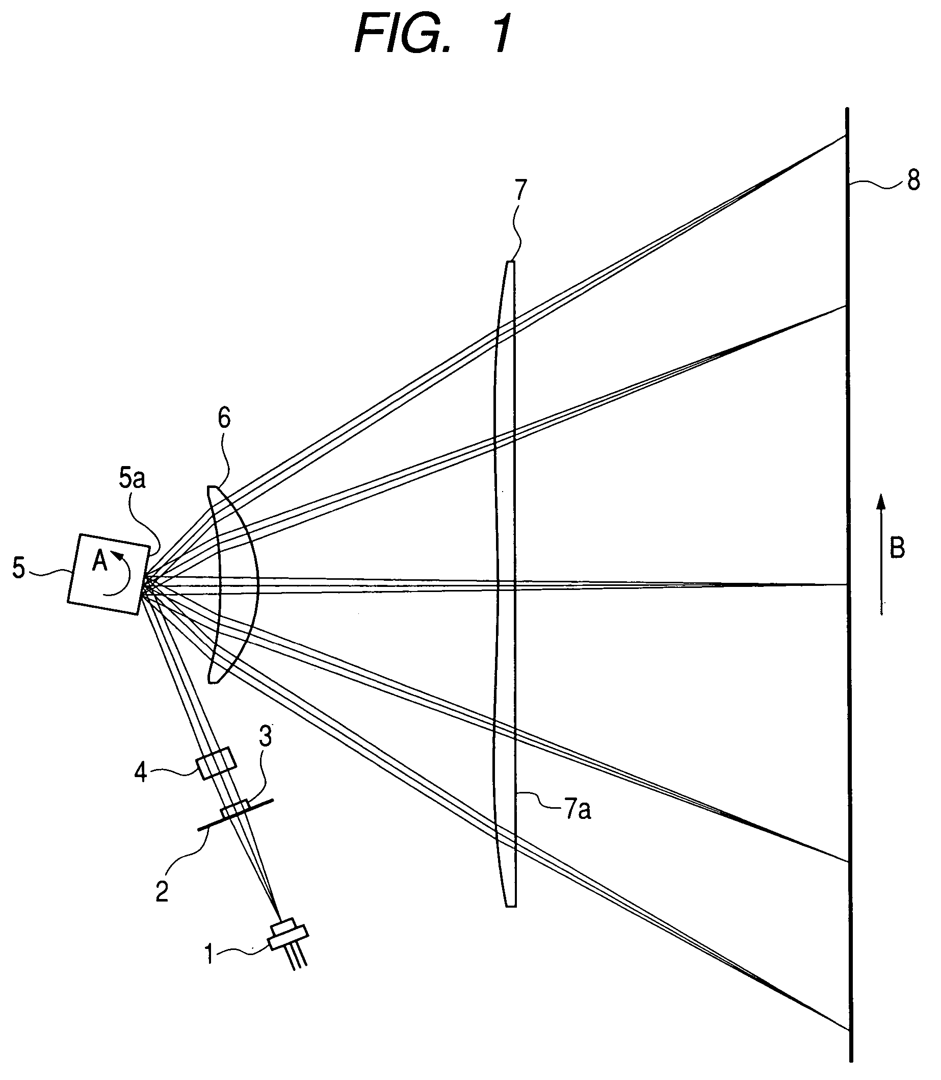
[0053]FIG. 1 is a main scanning sectional view showing an optical scanning device according to a first embodiment of the present invention.

[0054]Here, a main scanning direction indicates a direction perpendicular to the rotational axis of deflecting means. A sub scanning direction indicates a direction parallel to the rotational axis of the deflecting means. In addition, a main scanning section indicates a plane which is parallel to the main scanning direction and includes the optical axes of a deflection optical element (lens) 6 and a diffraction optical element (lens) 7 having a diffraction grid 7a formed on an exit surface of a diffraction part, which compose a scanning optical system.

[0055]A divergent light flux emitted from a single beam semiconductor laser 1 serving as light source means is limited by a diaphragm 2 so as to reduce a width of the light flux, thereby obtaining a desirable spot size. Then, the light flux is converted into a substantially p...

second embodiment

[0094](Second Embodiment)

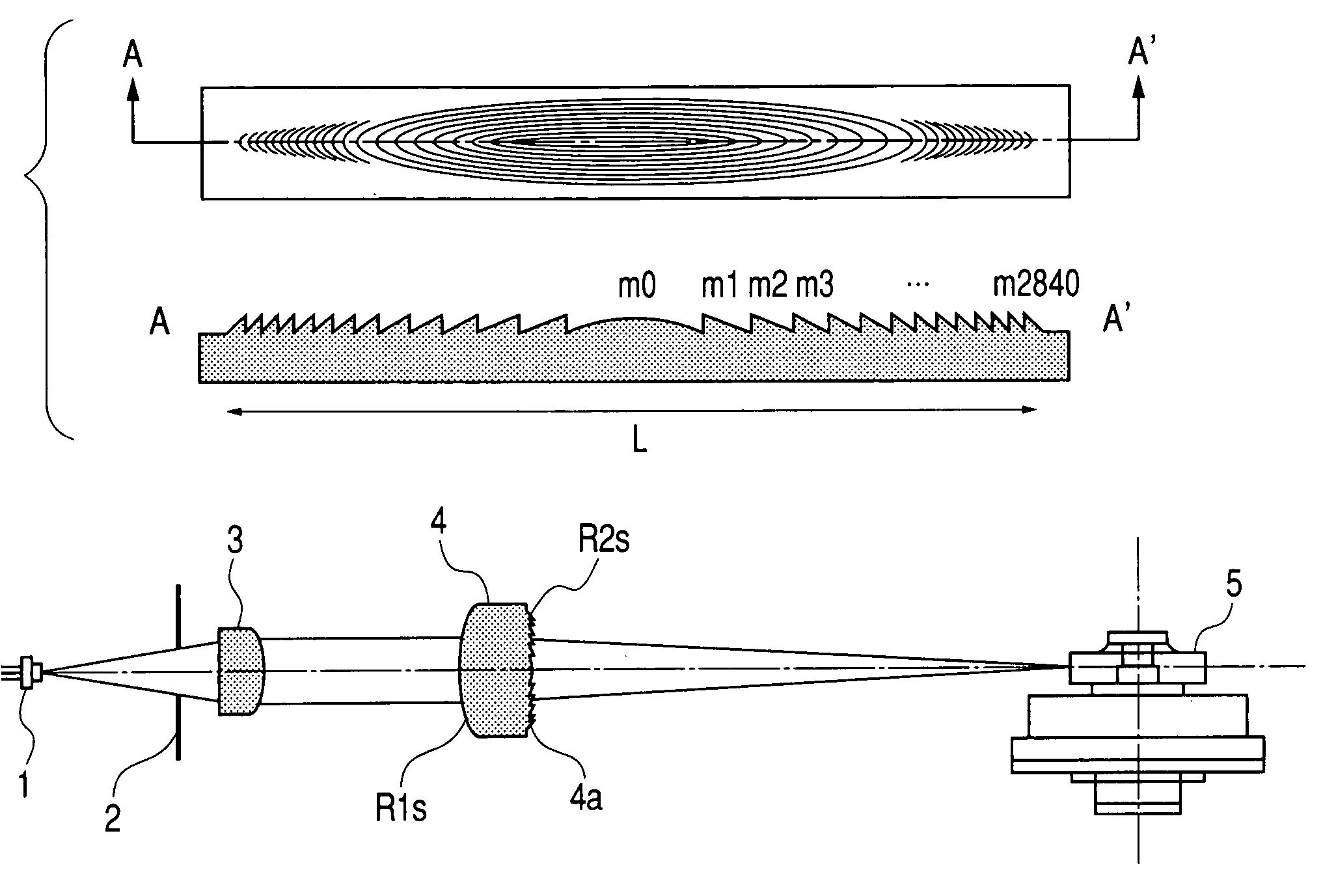
[0095]FIG. 8 is an explanatory view showing an optical scanning device according to a second embodiment of the present invention, which shows an embodiment in which a diffraction grid is formed in the cylinder lens 4. In this embodiment, a diffraction grid 4a is formed on an exit surface side of the cylinder lens 4 and has power in only the sub scanning direction. The cylinder lens 4 itself is made of an optical resin and can be produced at low cost by injection molding.

[0096]Table 4 shows curvatures of the cylinder lens 4, phase coefficients of the diffraction grid 4a, and the like.

[0097]The phase function used here is the same as in the first embodiment.

φ=2πk / λ·d0·Z2 (k=2 and λ=405 nm)

[0098]In this embodiment, the diffraction grid 4a is constructed using the second design order as in the first embodiment.

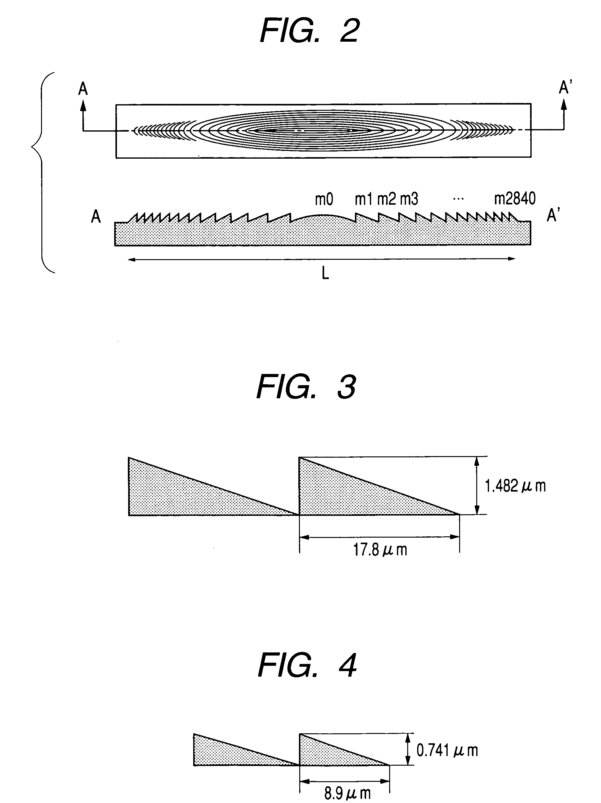
[0099]With respect to the diffraction grid used here, m·L·λ=111 and P / λ=56.35. Therefore, both Expression 1 and Expression 2 are satisfied. When the prese...

third embodiment

[0103](Third Embodiment)

[0104]FIG. 9 is an explanatory view showing a part of an optical scanning device according to a third embodiment of the present invention, which shows an embodiment in which a diffraction grid is formed in the collimator lens 3. In this embodiment, a diffraction grid 3a is formed on an incident surface side of the collimator lens 3. Because of a concentric diffraction grid, although the single collimator lens is used, it becomes an optical system in which an on-axis chromatic aberration is corrected.

[0105]Table 5 shows curvatures of the collimator lens 3, phase coefficients of the diffraction grid 3a, and the like.

[0106]The phase function used here is the same as in the first embodiment.

φ=2πk / λ·c0·H2, H2=Y2+Z2 (k=2 and λ=405 nm)

[0107]In this embodiment, the diffraction grid 3a is constructed using the second design order as in the first and second embodiments.

[0108]With respect to the diffraction grid 3a used here, m·L·λ=47 and P / λ=129.60. Therefore, both Exp...


PUM


Abstract

There is provided a diffraction grid which is easily produced without reducing a grid size. There is provided an optical scanning device having effects such as a chromatic aberration correction and a temperature compensation even when a short wavelength light source having a wavelength of 500 nm or less is used, and an image forming apparatus using the optical scanning device. In the optical scanning device having the diffraction grid, for which the short wavelength light source having a wavelength of 500 nm or less is used, a design order of the diffraction grid is set to a diffraction order equal to or larger than a second order to obtain a grid shape which is easily formed.

Description

BACKGROUND OF THE INVENTION[0001]1. Field of the Invention[0002]The present invention relates to an optical scanning device and an image forming apparatus using the same. In particular, the present invention relates to an optical scanning device that is suitably used for an apparatus such as a laser beam printer or a digital copying machine having an electrophotographic process, in which a light flux optically modulated and emitted from light source means is reflected and deflected on a polygon mirror serving as optical deflection means and then a surface to be scanned is scanned with the light flux through a scanning optical system to record image information. The present invention relates to an optical scanning device capable of providing a satisfactory image by adopting a diffraction grid for correction of chromatic aberration of magnification or temperature compensation and to an image forming apparatus using the same. In addition, the present invention relates to a color image ...

Claims


Application Information

Patent Timeline
Patent Type & Authority Patents(United States)
IPC IPC(8): B41J27/00G02B5/18B41J2/44G02B26/10G02B27/00G03G15/04H01J3/14H01J5/16
CPCG02B5/1852G02B27/0031G02B27/0037G02B27/4211G02B27/4227G02B27/4283G02B27/4294
Inventor SHIMOMURA, HIDEKAZUTANIMURA, KEN
Owner CANON KK
Why Eureka
Try Eureka