Phase-change recording material and information recording medium
a recording material and phase change technology, applied in the field of phase change recording materials and information recording media, can solve the problems of difficult to satisfy, significant noise of optical information recording medium, and significant noise of optical information recording medium, and achieve the effect of excellent recording signal characteristics and high storage stability of recording signals
- Summary
- Abstract
- Description
- Claims
- Application Information
AI Technical Summary
Benefits of technology
Problems solved by technology
Method used
Image
Examples
examples
[0329]Now, the present invention will be explained with reference to Examples wherein the phase-change recording material to be used in the present invention is applied to an optical information recording medium. However, the present invention is by no means restricted to the application to an optical information recording medium within a range not to exceed the gist of the present invention.
[0330]In the following Examples, an optical information recording medium may be referred to simply as “a disk”, “an optical disk”, “a phase-change type optical disk” etc. in some cases.
reference example 1
[0373]A disk of Reference Example 1 was prepared as follows.
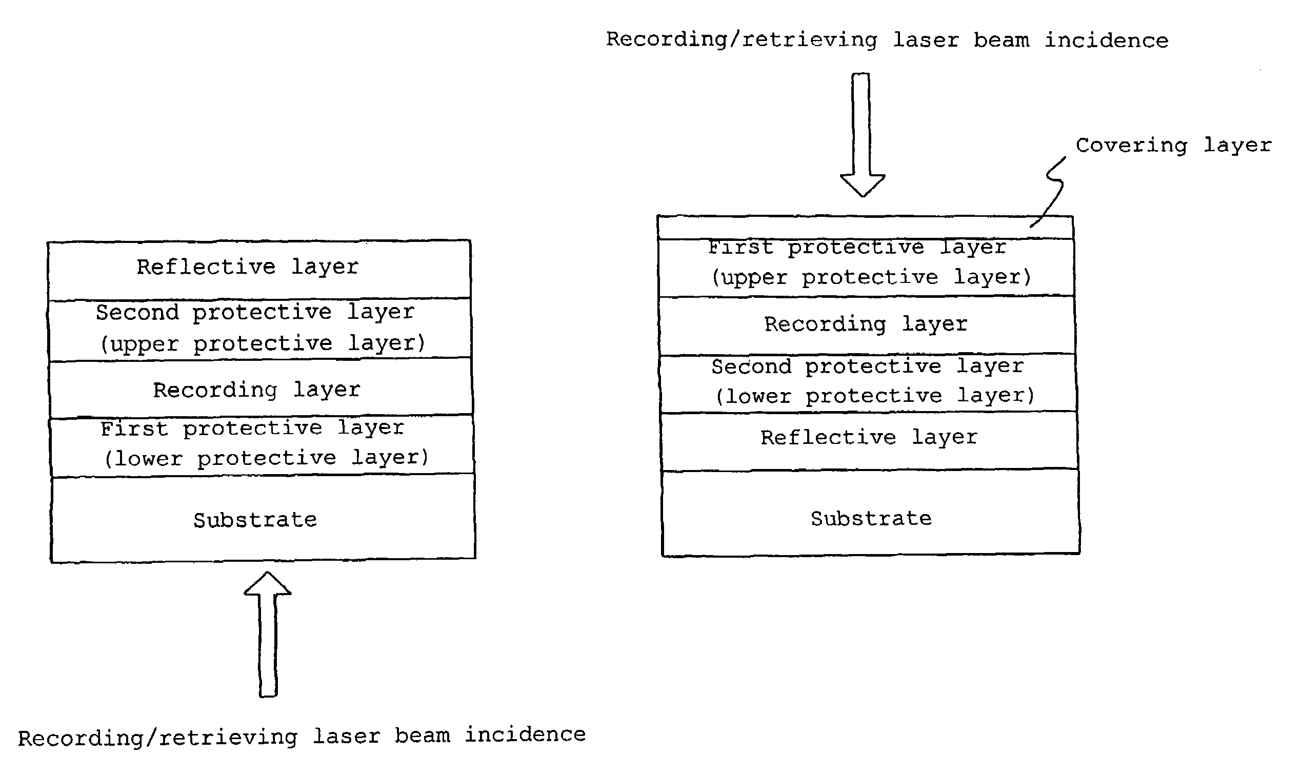
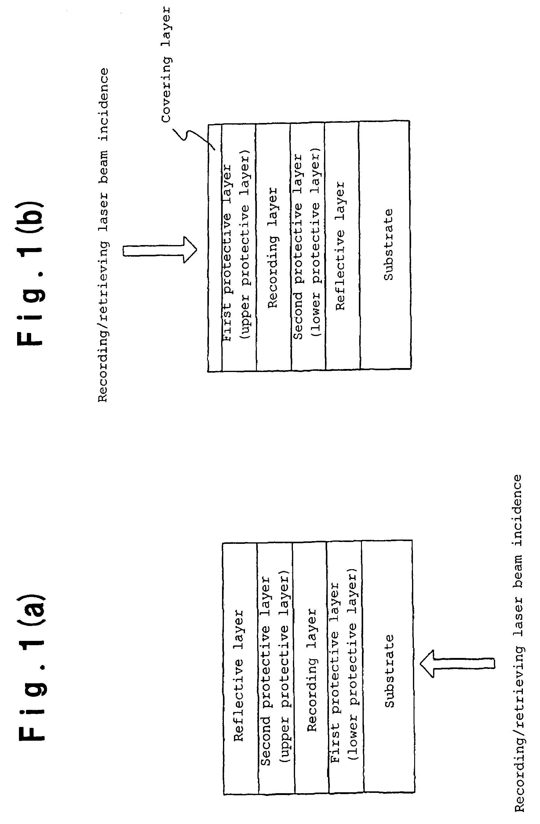
[0374]On a disk-shape polycarbonate substrate having a diameter of 120 mm and a thickness of 1.2 mm and having guide grooves with a groove width of 0.5 μm, a groove depth of 40 nm and a groove pitch of 1.6 μm, first to fifth layers were formed in order by a sputtering method as follows. The first layer is a (ZnS)80(SiO2)20 protective layer, the second layer is a recording layer, the third layer is a (ZnS)80(SiO2)20 protective layer, the fourth layer is a Ta interfacial layer, and the fifth layer is a Ag reflective layer. A protective layer comprising an ultraviolet-curing resin was further formed on these layers to prepare a phase-change type optical disk. The film thicknesses of the respective layers and the values x, y, z and w when the recording layer composition is represented by Gex(InwSn1-w)yTezSb1-x-y-z are shown in Table 2. Then, initial crystallization was carried out under the same conditions as in Example 1.
[0375...
examples 13 and 14
[0403]A polycarbonate resin substrate having a thickness of 0.6 mm and a track pitch of 0.74 μm was formed by injection molding and employed for the following experimental examples. Of the groove formed on the substrate, the groove width was about 0.31 μm, and the groove depth was about 28 nm. The groove shape was obtained by an optical diffraction method by U-groove approximation by means of a He—Cd laser beam having a wavelength of 441.6 nm.
[0404]Then, on the substrate, a (ZnS)80 (SiO2)20 protective layer of 40 nm, a (Y2O2S)90(ZnO)10 layer of 2 nm, a Ge7In6Sbs6Sn24Te7 recording layer of 10 nm, a (Y2O2S)90(ZnO)10 layer of 14 nm, a Ta interfacial layer of 2 nm, a Ag reflective layer of 200 nm and an ultraviolet-curing resin layer of about 4 μm were formed in this order. The Ta layer is an interfacial layer to prevent diffusion of S into the Ag reflective layer.
[0405]Formation of the respective layers was carried out by sequential deposition by a sputtering method on the substrate wi...
PUM
| Property | Measurement | Unit |
|---|---|---|
| thickness | aaaaa | aaaaa |
| thickness | aaaaa | aaaaa |
| thickness | aaaaa | aaaaa |
Abstract
Description
Claims
Application Information
 - R&D
- Intellectual Property
- Life Sciences
- Materials
- Tech Scout
- Unparalleled Data Quality
- Higher Quality Content
- 60% Fewer Hallucinations
Browse by: Latest US Patents, China's latest patents, Technical Efficacy Thesaurus, Application Domain, Technology Topic, Popular Technical Reports.
© 2025 PatSnap. All rights reserved.Legal|Privacy policy|Modern Slavery Act Transparency Statement|Sitemap|About US| Contact US: help@patsnap.com


