
On-chip differential multi-layer inductor

Inactive Publication Date: 2006-08-15
AVAGO TECH INT SALES PTE LTD
View PDF7 Cites 29 Cited by
  • Summary
  • Abstract
  • Description
  • Claims
  • Application Information

AI Technical Summary

Benefits of technology

[0011]In another aspect of an on-chip differential multi-layer inductor, the windings on multiple layers may have similar metalization (i.e., have about the same amount of metal layers). The amount of metalization, the geometric shape of the windings, and the number of layers to use may be determined based on the desired inductance value, desired metalization coverage, and operating rates. By evenly distributing or near evenly distributing metalization amongst the layers, the manufacturing yield of integrated circuits including on-chip inductors is increased.

Problems solved by technology

In general, on-chip inductors' performance criteria is becoming more and more demanding as the demands for larger inductance values, high Q factors, lower noise levels, higher operating rates, et cetera increase.
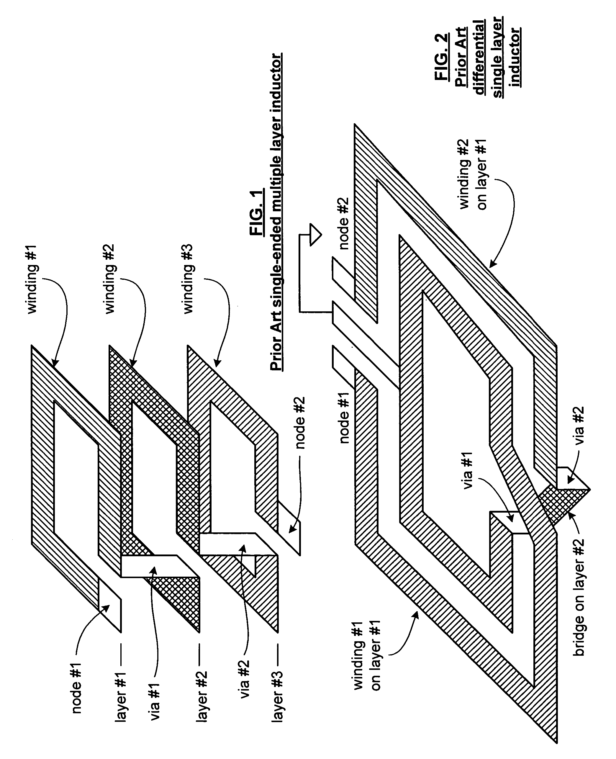
While such an inductor provides a relatively small footprint and can have higher inductance values than single layer inductors of a similar footprint, it typically has a relatively significant capacitance value that limits the resonant frequency, which in turn limits the operating frequency of the inductor.
Such a differential inductor has a low capacitance value, but to achieve a large inductance value, it consumes a significant amount of IC real estate.

Method used


Image

  • On-chip differential multi-layer inductor
  • On-chip differential multi-layer inductor
  • On-chip differential multi-layer inductor

Examples


Embodiment Construction

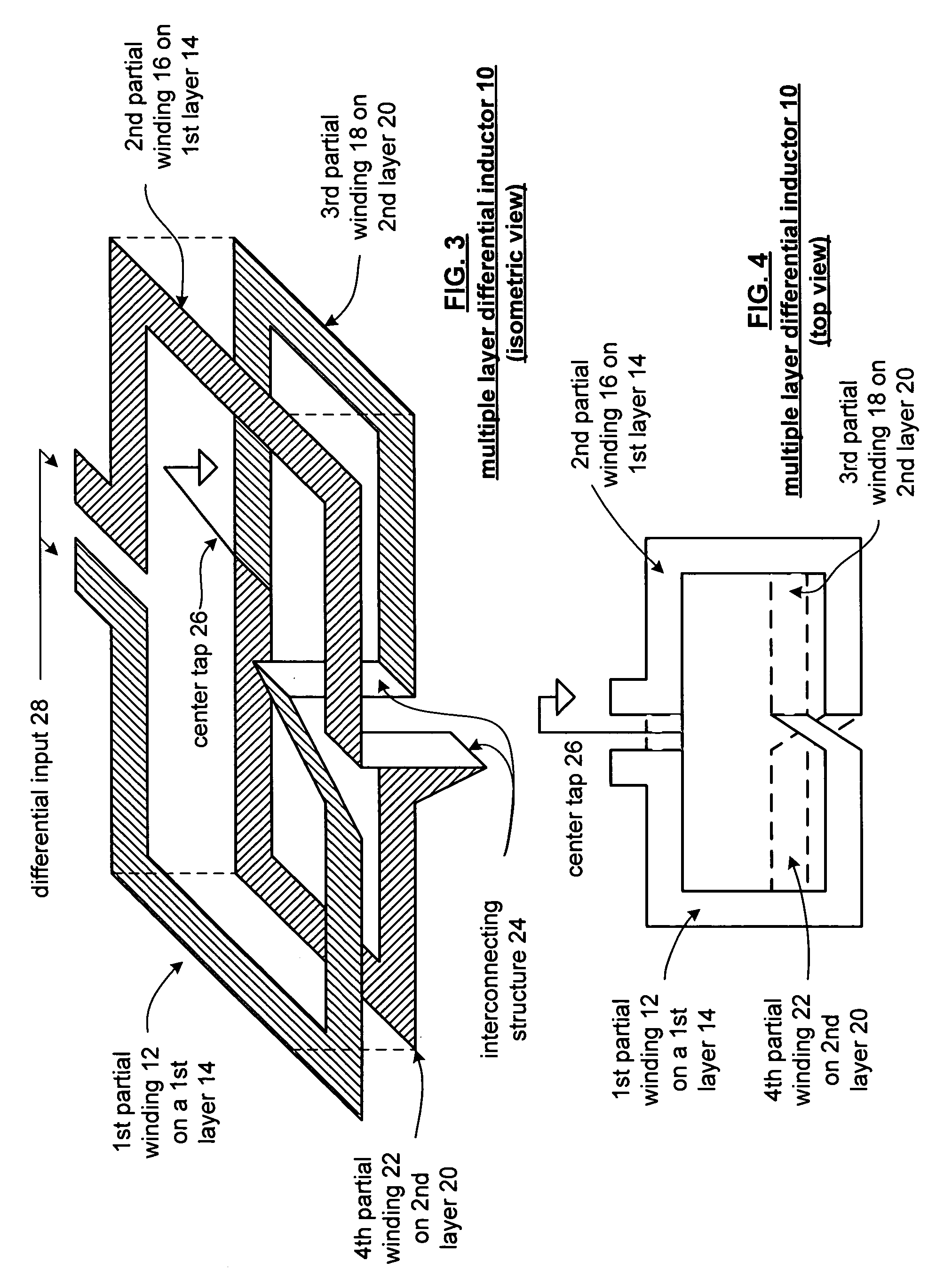
[0023]FIG. 3 illustrates an isometric view of a multiple layer differential inductor 10 that includes a 1st partial winding 12 on a 1st layer 14 of an integrated circuit, a 2nd partial winding 16 on the 1st layer 14, a 3rd partial winding 18 on a 2nd layer 20 of the integrated circuit, a 4th partial winding 22 on the 2nd layer 20, an interconnecting structure 24, and a center tap 26. The 1st and 2nd partial windings 12 and 16 are operably coupled to receive a differential input 28. As can be seen in FIG. 3, the 1st partial winding 12 is coupled to the 3rd partial winding 18 by the interconnecting structure 24. Similarly, the 2nd partial winding 16 is coupled to the 4th partial winding 22 via the interconnecting structure 24. The 4th partial winding 22 and the 3rd partial winding 18 are both coupled to center tap 26. As configured, the winding formed by the 1st partial winding and 3rd partial winding 18 is identical (within manufacturing limits) to the winding formed by the 2nd parti...


PUM

PropertyMeasurementUnit
Lengthaaaaaaaaaa
Fractionaaaaaaaaaa
Thicknessaaaaaaaaaa

Abstract

An on-chip differential multi-layer inductor includes a 1st partial winding on a 1st layer, a 2nd partial winding on the 1st layer, a 3rd partial winding on a 2nd layer, a 4th partial winding on the 2nd layer, and an interconnecting structure. The 1st and 2nd partial windings on the 1st layer are operably coupled to receive a differential input signal. The 3rd and 4th partial windings on the 2nd layer are each operably coupled to a center tap. The interconnecting structure couples the 1st, 2nd, 3rd and 4th partial windings such that the 1st and 3rd partial windings form a winding that is symmetrical about the center tap with a winding formed by the 2nd and 4th partial windings. By designing the on-chip differential multi-layer inductor to have a desired inductance value, a desired Q factor, and a desired operating rate, a desired resonant frequency and corresponding desired capacitance value can be determined. Having determined the electrical parameters of the multi layer established, the geometric shapes of the windings, number of windings, number of layers to support the inductor, and the interconnecting structure may be determined.

Description

[0001]This patent application is claiming priority under 35 USC § 120 to co-pending patent application entitled ON-CHIP DIFFERENTIAL MULTI-LAYER INDUCTOR having a Ser. No. of 10 / 161,518 and a filing date of Jun. 3, 2002.TECHNICAL FIELD OF THE INVENTION[0002]This invention relates generally to integrated circuits and more particularly to on-chip inductors.BACKGROUND OF THE INVENTION[0003]As is known, wireless communication standards place stringent requirements on wireless communication devices' dynamic range of operation to accommodate for the dramatic variations in signal strength of receive signals, which may vary by orders of magnitude. To meet these requirements, wireless communication devices are designed using radio frequency (RF) integrated circuits (IC) that consume low power and produce little noise. As is also known, on-chip inductors are significant components of RFIC's and are used in oscillators, impedance matching networks, emitter degeneration circuits, filters, and / o...

Claims


Application Information

Patent Timeline
IPC IPC(8): H01F5/00H01F17/00H01F21/12H01L21/02H01L23/522H01L27/08
CPCH01F17/0013H01F21/12H01L27/08H01L28/10H01L23/5227H01F2021/125Y10T29/4902H01L2924/3011H01L2924/0002H01L2924/00
Inventor KYRIAZIDOU, CHRYSSOULA
Owner AVAGO TECH INT SALES PTE LTD
Learn More