ECC based system and method for repairing failed memory elements

a memory element and ecc technology, applied in information storage, static storage, digital storage, etc., can solve the problems of tens of hours of burn-in testing to manifest all early life failures, the problem is presented for production verification of the completed integrated circuit, and the failure of marginal dram elements only later

Inactive Publication Date: 2006-08-01
IBM CORP
View PDF24 Cites 31 Cited by
  • Summary
  • Abstract
  • Description
  • Claims
  • Application Information

AI Technical Summary

Benefits of technology

[0011]At some appropriate time, which can be ongoing during operation, or scheduled upon a power-down or power-up sequence, failure patterns are automatically identified by first logic circuits based on the recorded locations. Examples of failure patterns include partial or full wordline failure and full or partial bitline failure. Based on the identif

Problems solved by technology

Traditional ASICs, having mainly logic circuits such as for a microprocessor and SRAM elements, are production tested in only a few minutes, because failures are manifested by relatively large defect currents (from several to several hundred microamps (>1×10E-6), which are manifested either before or after very short durations of high stress testing.
On the other hand, it may take tens of hours of burn-in testing to manifest all early life failures within a DRAM because of much smaller tolerances for defect currents, which typically measure in sub-picoamps (<1×10E-12).
Thus, when a DRAM macro is embedded into an ASIC, a problem is presented for production verifying the completed integrated circuit.
Instead, such marginal DRAM elements will only fail

Method used


Image

  • ECC based system and method for repairing failed memory elements
  • ECC based system and method for repairing failed memory elements
  • ECC based system and method for repairing failed memory elements

Examples


Embodiment Construction

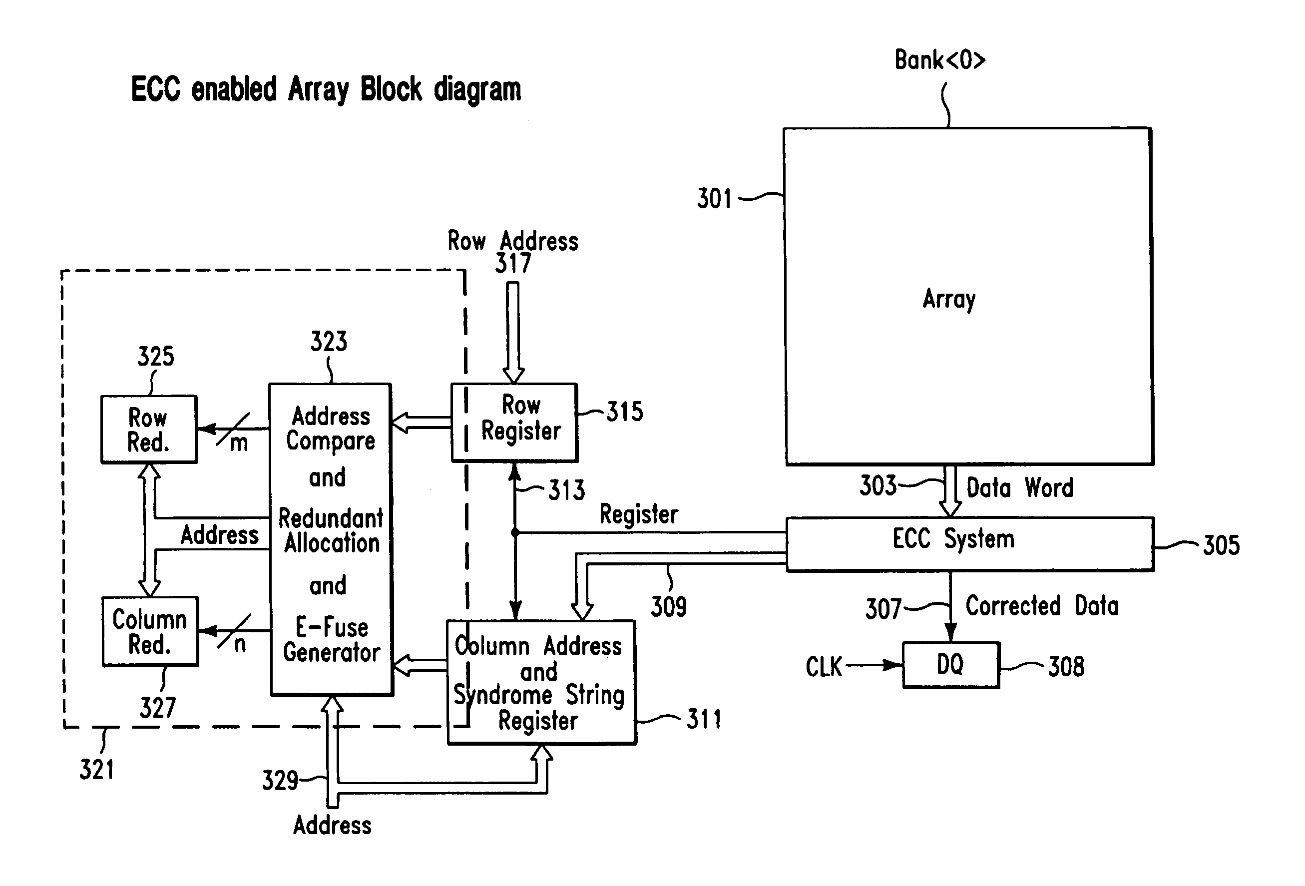
[0015]FIG. 3 illustrates a preferred arrangement for implementing the present invention in the context of a DRAM, although the invention could be implemented with another memory type such as SRAM or EEPROM. As shown in FIG. 3, a DRAM, either standalone or preferably embedded within an ASIC, includes a Bank of memory cells arranged within an array 301.

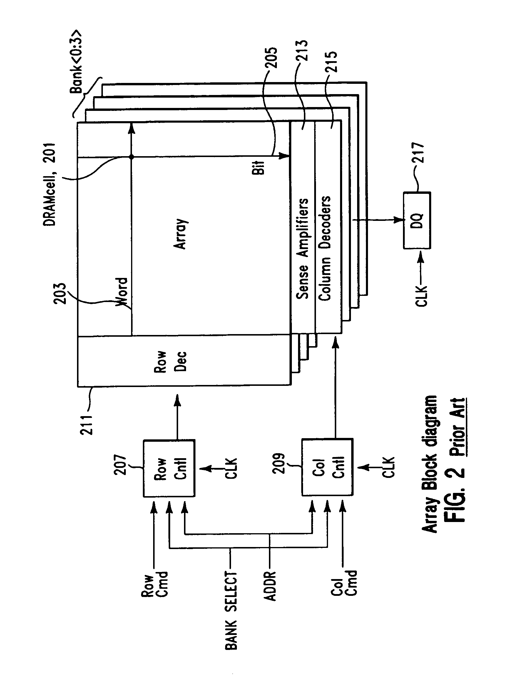
[0016]Memory cells within array 301 are accessed by an address and commands in the manner described above relative to FIG. 2. Circuitry which selects row, column, and bank, as well as associated control circuitry and sense amplifiers are not shown in FIG. 3 but are understood to be present, as described above relative to FIG. 2. During a read operation, retrieved information from a row or partial row of memory cells in array 301 is output from sense amplifiers (not shown) associated with Bank as a data word 303 to an ECC system 305. Typically, a row of memory cells is accessed by a wordline using a row address. A plurality of data words...


PUM


Abstract

An ECC based system and method within an integrated circuit memory for self-repair of a failed memory element is disclosed. The method includes processing, within the integrated circuit, data and check bits retrieved from addressed memory locations therein. The locations of memory failures are automatically recorded within the integrated circuit. Logic circuits within the integrated circuit automatically identify failure patterns based on the locations. Based on the identified failure patterns, logic circuits within the integrated circuit then permanently replace a failed memory element with an appropriate redundancy element, using devices such as electronic fuse or antifuse. In this manner, the integrated circuit automatically identifies and effects self repair of a failed memory element therein.

Description

FIELD OF THE INVENTION[0001]The present invention relates to dynamic random access memories (DRAMs) including DRAMs embedded in multi-purpose integrated circuits. More specifically, the invention relates to a system and method for repairing a failed memory element.BACKGROUND OF THE INVENTION[0002]Recently, designers of ASICs (Application Specific Integrated Circuits) have expressed interest in incorporating DRAM macros to enhance on-chip storage density. Greater processing widths and speed available now to ASICs is beginning to demand storage densities which stretch the limits of static random access memory (SRAM), which has traditionally been embedded in those ASICs which include a processor element such as a microprocessor.[0003]Owing to their diverse circuit implementations and design goals, production verification testing of ASICs and DRAMs has differed widely. Traditional ASICs, having mainly logic circuits such as for a microprocessor and SRAM elements, are production tested i...

Claims


Application Information

Patent Timeline
IPC IPC(8): G11C29/00G11C29/42
CPCG11C29/42G11C29/72G11C2029/4402G11C29/789
Inventor BARTH, JR., JOHN E.ELLIS, WAYNE F.FIFIELD, JOHN A.
Owner IBM CORP
Why Eureka
Try Eureka