Interconnect line selectively isolated from an underlying contact plug

a contact plug and interconnect line technology, applied in the field of semiconductor devices, can solve the problems of increasing the potential for shorting between adjacent electrical conductors, the close proximity of discrete electrical features within memory cells, and the problem of integrating circuit designers facing problems related to each other, so as to achieve efficient connection of interconnect lines and maintain electrical isolation. the effect of high integration

Inactive Publication Date: 2006-06-13
MICRON TECH INC
View PDF34 Cites 12 Cited by
  • Summary
  • Abstract
  • Description
  • Claims
  • Application Information

AI Technical Summary

Benefits of technology

The present invention relates to a method for selectively connecting an electrical interconnect line with an associated contact to an active area and electrically isolating the interconnect line from other underlying contacts for other electrical features. This allows the electrical features to be formed in closer proximity to one another for higher levels of integration. The invention also provides a method for efficiently connecting interconnect lines to a plurality of selected epitaxial silicon contact studs while maintaining electrical isolation from other non-selected plugs.

Problems solved by technology

Modern integrated circuit designers confront problems related to the need for increasingly smaller size and higher levels of integration.
This increasingly close proximity of the discrete electrical features within a memory cell, such as a dynamic random access memory (DRAM) cell, becomes problematic in view of the increasing potential for shorting between adjacent electrical conductors.
This shorting may cause a memory cell to function improperly or not at all.
An additional concern relating to the manufacture of integrated circuits is the increasing complexity and cost related to the necessity for diminishing size of the memory devices.
Additionally, crystalline or contaminate defects in the conductive areas of an integrated circuit can deteriorate its operation.

Method used


Image

  • Interconnect line selectively isolated from an underlying contact plug
  • Interconnect line selectively isolated from an underlying contact plug
  • Interconnect line selectively isolated from an underlying contact plug

Examples


Embodiment Construction

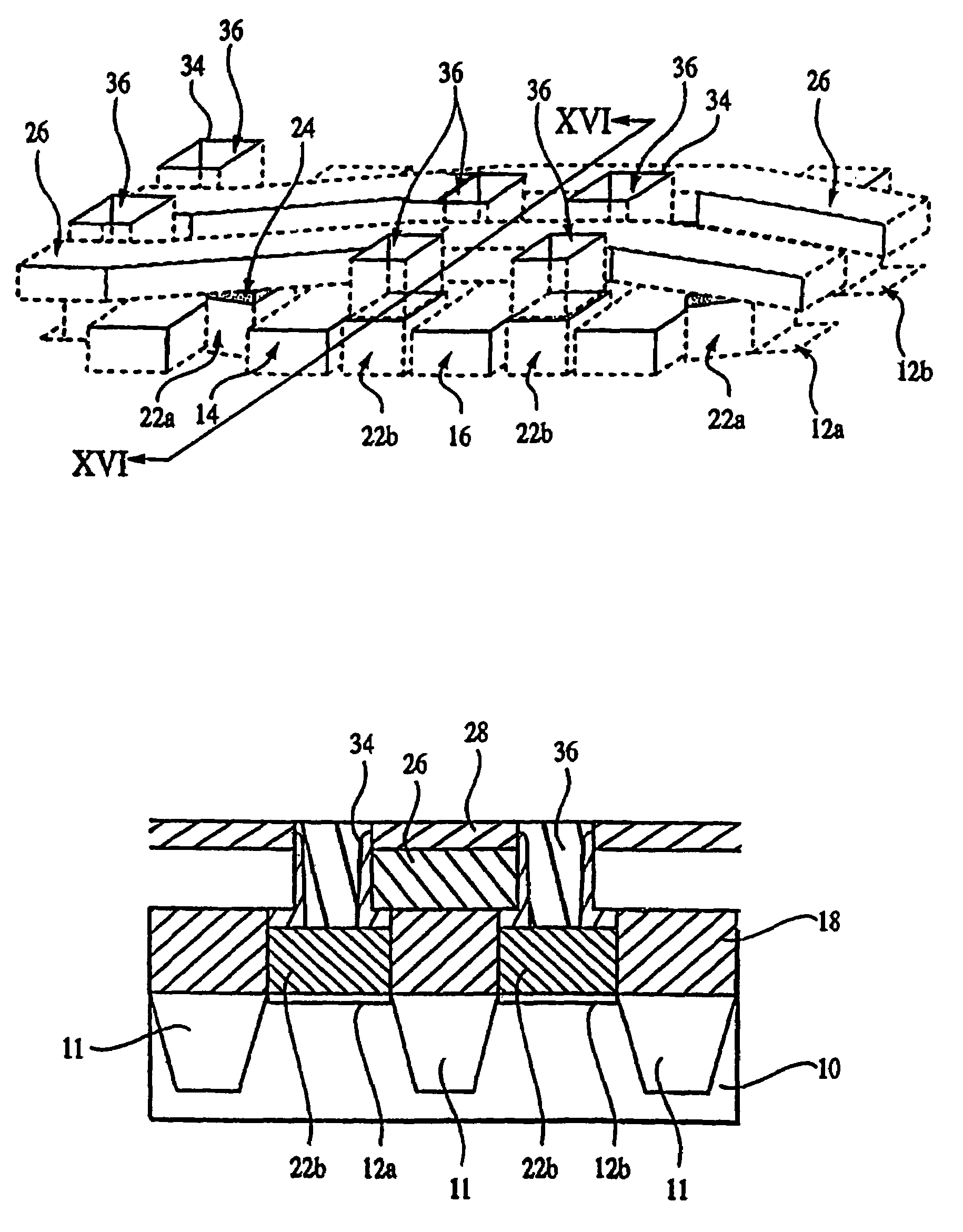
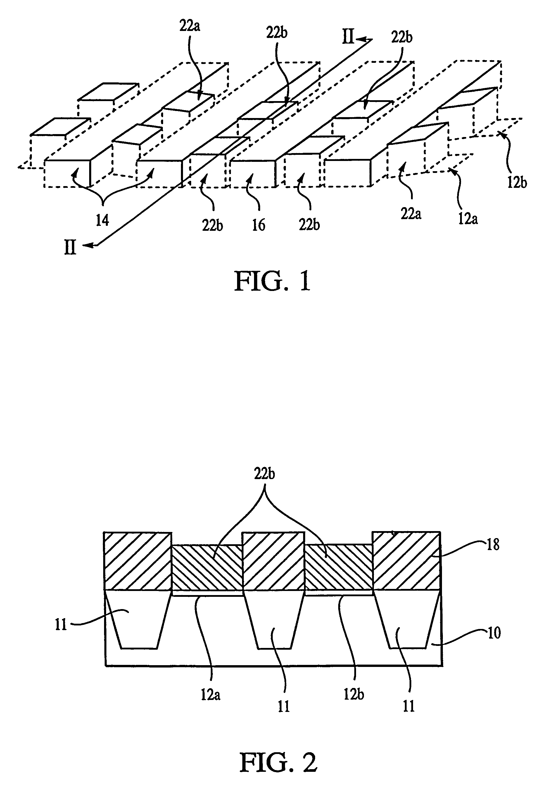
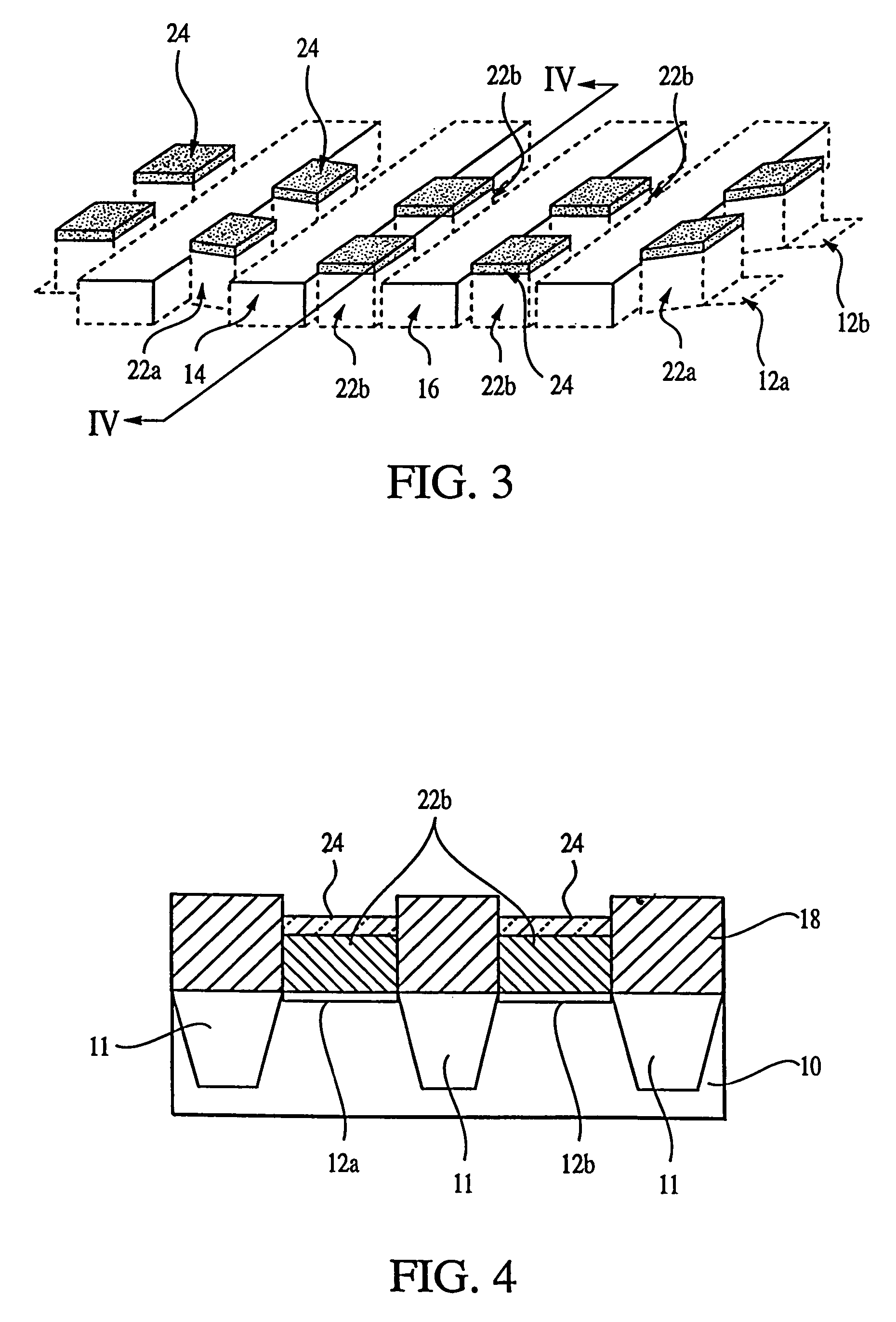
[0023]DRAM memory circuits are currently the most popular type of memory circuits used as the main memory of processor-based systems. Therefore, the invention will be discussed in connection with DRAM memory circuits for simplicity sake. However, the invention herein disclosed has broader applicability and is not limited only to DRAM memory circuits. It may be used in any other type of memory circuit, such as SRAM (static random access memory), MRAM (magnetoresistive random access memory), Flash, and PCRAM (programmable conductor random access memory), etc., as well as in any other circuit in which electrical contacts are formed in close proximity to, and intended to be insulated from, other circuit devices.

[0024]Also, the terms “wafer” and “substrate” are used interchangeably and are to be understood as including silicon, silicon-on-insulator (SOI), and silicon-on-sapphire (SOS) technology, doped and undoped semiconductors, and other semiconductor structures. Furthermore, reference...


PUM


Abstract

The present invention relates to selectively electrically connecting an electrical interconnect line, such as a bit line of a memory cell, with an associated contact stud and electrically isolating the interconnect line from other partially underlying contact studs for other electrical features, such as capacitor bottom electrodes. The interconnect line can be formed as initially partially-connected to all contact studs, thereby allowing the electrical features to be formed in closer proximity to one another for higher levels of integration. In subsequent steps of fabrication, the contact studs associated with memory cell features other than the interconnect line can be isolated from the interconnect line by the removal of a silicide cap, or the selective etching of a portion of these contact studs, and the formation of an insulating sidewall between the non-selected contact stud and the interconnect line.

Description

[0001]This application is a divisional of U.S. patent application Ser. No. 10 / 303,880, filed Nov. 26, 2002, now U.S. Pat. No. 6,713,378, which is a continuation-in-part of U.S. patent application Ser. No. 09 / 595,922, filed Jun. 16, 2000, now U.S. Pat. No. 6,511,879, the entirety of each is hereby incorporated by reference herein.BACKGROUND OF INVENTION[0002]1. Field of the Invention[0003]This invention relates to a semiconductor device and a method of manufacturing such a device, wherein signal lines (e.g., bit lines of a memory device, etc.) may be isolated from adjacent electrical conductors.[0004]2. Discussion of the Related Art[0005]Modern integrated circuit designers confront problems related to the need for increasingly smaller size and higher levels of integration. In the art of integrated circuit fabrication, and particularly when dealing with modern memory circuits, circuit manufacturers must design memory cells that are more densely constructed such that the basic elements...

Claims


Application Information

Patent Timeline
Patent Type & Authority Patents(United States)
IPC IPC(8): H01L27/108H01L21/285H01L21/4763H01L21/768H01L29/76H10B12/00
CPCH01L21/28525H01L21/76801H01L21/76802H01L21/76831H01L21/76837H01L21/76889H01L21/76895H01L27/10814H01L27/10855H01L21/76885H01L27/10888H01L27/10885H10B12/315H10B12/0335H10B12/482H10B12/485
Inventor DRYNAN, JOHN M.
Owner MICRON TECH INC
Why Eureka
Try Eureka