Group III nitride compound semiconductor device

Inactive Publication Date: 2006-05-09
TOYODA GOSEI CO LTD
View PDF25 Cites 11 Cited by
  • Summary
  • Abstract
  • Description
  • Claims
  • Application Information

AI Technical Summary

Benefits of technology

[0013]According to the Group III nitride compound semiconductor device configured as described above, the farthest point of the p electrode from the n electrode is within the aforementioned distance. Hence, even in the case where the resistance of an n-type semiconductor layer is high, electrons are sufficiently injected into the farthest device portion from the n electrode (electric current is diffused). As a result, light is emitted more evenly from the whole surface of the device.
[0019]Since the n auxiliary electrode is present in the central portion of the device, the distance from the n auxiliary electrode to any corner portion of the device is kept constant. Hence, reduction in luminous output from the corner portions can be prevented.
[0026]Since the p auxiliary electrode is present in the central portion of the translucent electrode, the distance from the p auxiliary electrode to any corner portion of the translucent electrode is kept constant. Hence, reduction in luminous output from the corner portions can be prevented.
[0027]In the Group III nitride compound semiconductor device having both the n electrode and the p electrode configured as described above, it is preferable that the n auxiliary electrode and the p auxiliary electrode are arranged like a comb in a plan view of the device. The device does not operate (the device does not emit light when the device is a light-emitting device) in certain portions of the n auxiliary electrode and the p auxiliary electrode. Hence, when the n auxiliary electrode and the p auxiliary electrode are arranged like a comb, the inoperative portions can be disposed as symmetrical or regular patterns in the device, so that the device can be used easily. In the case of a light-emitting device, light can be taken out evenly.
[0028]In the Group III nitride compound semiconductor device having both the n electrode and the p electrode configured as described above, it is preferable that the n auxiliary electrode and the p auxiliary electrode include portions arranged in parallel with each other in a plan view of the device. The device does not operate (the device does not emit light when the device is a light-emitting device) in certain portions of the n auxiliary electrode and the p auxiliary electrode. Hence, when the parallel portions are disposed, the inoperative portions can be disposed as symmetrical or regular patterns in the device, so that the device can be used easily. In the case of a light-emitting device, light can be taken out evenly.
[0031]If the electric power consumed by the light-emitting device increases because of increase in the chip size of the light-emitting device, there arises a problem of burning between the p seat electrode and the translucent electrode in addition to the aforementioned problem. It is therefore preferable that a p auxiliary electrode is provided to extend from the p seat electrode. When the p auxiliary electrode is provided, a sufficient area can be obtained between the p seat electrode and the translucent electrode and between the p auxiliary electrode and the translucent electrode to thereby prevent occurrence of the burning. Hence, the amount of current (permissible current quantity) allowed to be applied to the p seat electrode increases, so that the amount of current required for emitting light from the whole surface of the device can be kept sufficiently.

Problems solved by technology

That is, even in the case where current density exceeding the predetermined value is injected, it is impossible to obtain increase in the luminous output in accordance with the current density.

Method used


Image

  • Group III nitride compound semiconductor device
  • Group III nitride compound semiconductor device
  • Group III nitride compound semiconductor device

Examples


Embodiment Construction

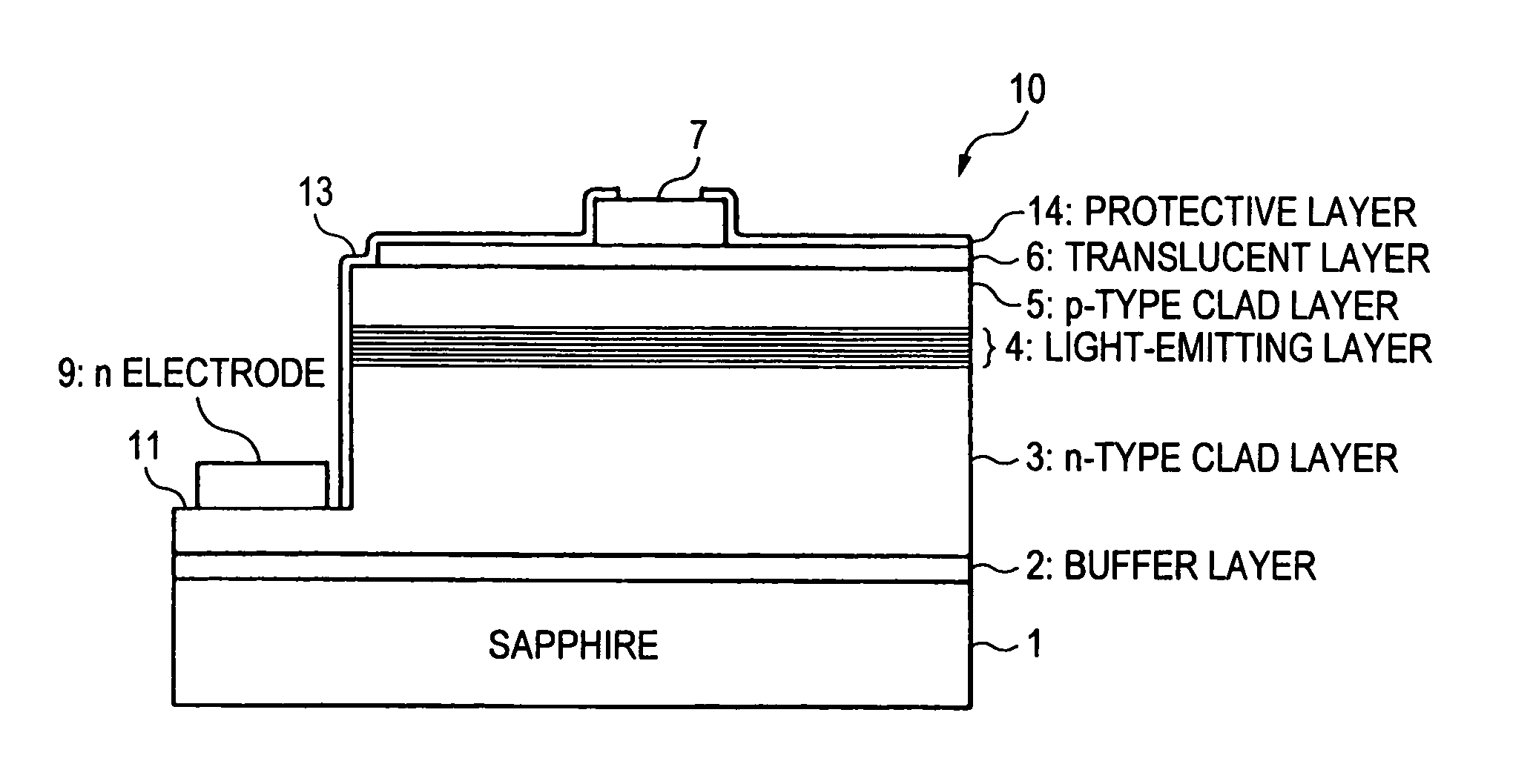
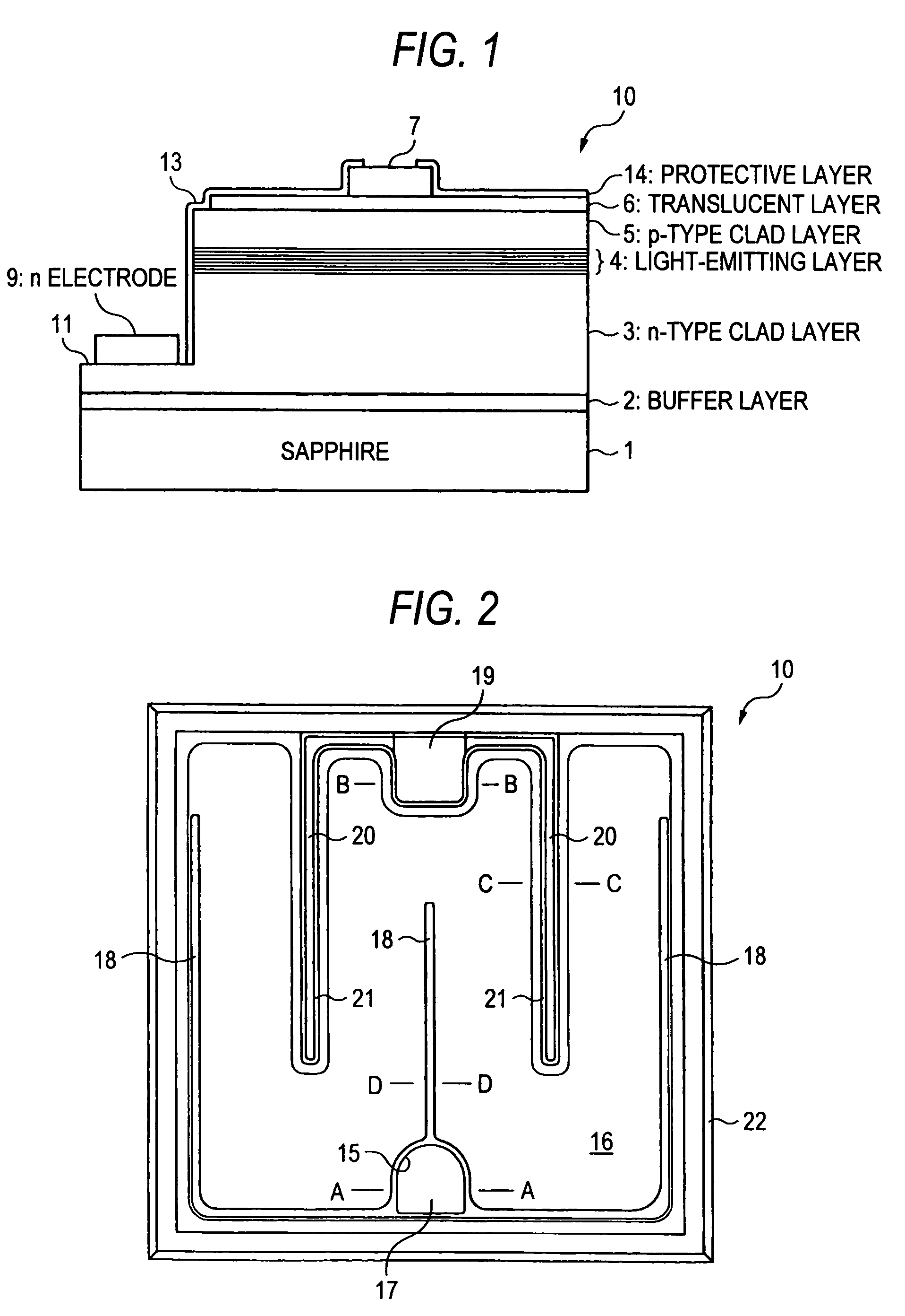
[0098]Respective members constituting the invention will be described below in detail taking a Group III nitride compound semiconductor light-emitting device as an example.

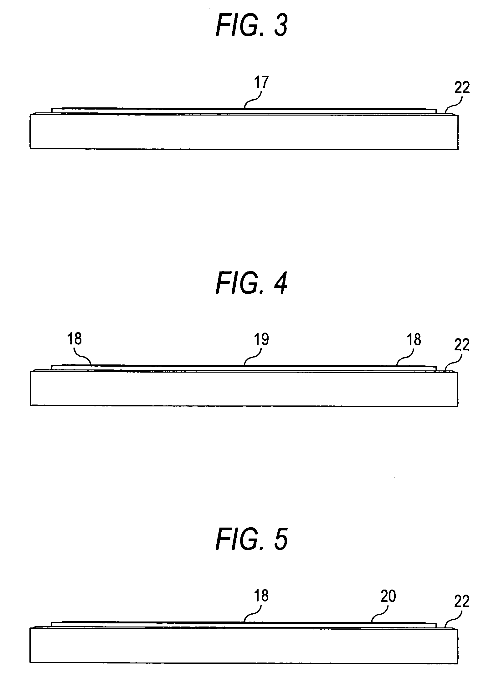
[0099]An n electrode is formed on an n contact layer revealed by etching a semiconductor layer. Although any material can be selected as the material of the n electrode if ohmic contact can be obtained between this material and the n-type Group III nitride compound semiconductor, an aluminum alloy such as a vanadium-aluminum alloy is preferably used.

[0100]The shape of the n electrode is also optional. According to an aspect of the invention, a combination of an n seat electrode and an n auxiliary electrode extended from the n seat electrode may be preferably used as the n electrode so that the distance from any point of a p electrode to the n electrode is selected to be in a predetermined range. The n seat electrode may be disposed in substantially the central portion of a side of the device or may be disposed in ...


PUM


Abstract

An object of the present invention is to provide a large-size light-emitting device from which uniform light emission can be obtained.That is, in the present invention, in a device having an outermost diameter of not smaller than 700 μm, a distance from an n electrode to a farthest point of a p electrode is selected to be not larger than 500 μm.

Description

[0001]The present Application is a Divisional Application of U.S. patent application Ser. No. 10 / 240,250 filed on Sep. 30, 2002. Now U.S. Pat. No. 6,777,805 which is a 371 of PCT / JP01 / 02758 Mar. 30, 2001.TECHNICAL FIELD[0002]The present invention relates to a Group III nitride compound semiconductor device. The invention is adapted for improvement in electrodes of a Group III nitride compound semiconductor light-emitting device such as a blue light-emitting diode.BACKGROUND ART[0003]In a Group III nitride compound semiconductor light-emitting device such as a blue light-emitting diode, various proposals have been made for obtaining uniform light emission from the whole surface of the device.[0004]For example, in Unexamined Japanese Patent Publication No. Hei. 8-340131 and Unexamined Japanese Patent Publication No. Hei. 10-117017, a p auxiliary electrode is provided radially on an upper surface of a p contact layer to attain uniformity of electric current density injected into the p ...

Claims


Application Information

Patent Timeline
IPC IPC(8): H01L23/48H01L33/32H01L33/38
CPCH01L33/32H01L33/38H01L24/05H01L33/20H01L2224/02166H01L2224/05552H01L2924/1301H01L2224/0603H01L2924/00H01L2924/181H01L2924/12042H01L2924/12041
Inventor UEMURA, TOSHIYAHIRANO, ATSUOOTA, KOICHINAGASAKA, NAOHISA
Owner TOYODA GOSEI CO LTD
Why Eureka
Try Eureka