Dynamic random access memory cell leakage current detector
a random access memory and leakage current technology, applied in the field of dynamic memory, can solve the problems of difficult to accurately detect or measure very small currents, leakage current is a serious problem for deep-submicron cmos devices, and the charge stored in the cell capacitor is not held very well
- Summary
- Abstract
- Description
- Claims
- Application Information
AI Technical Summary
Benefits of technology
Problems solved by technology
Method used
Image
Examples
embodiment 200
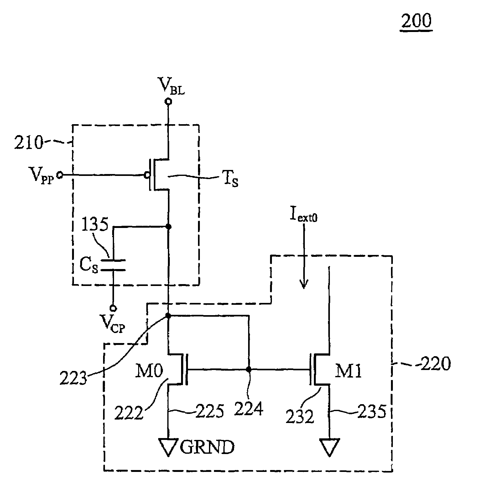
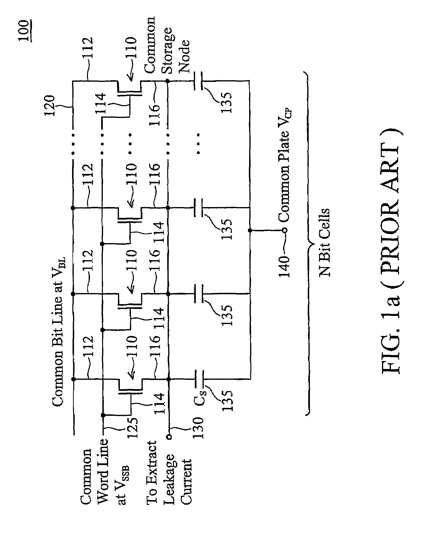
[0025]While there is no requirement as to how many cells need to be in “0” state cell array 210, it is advantageous that the magnitude of the leakage currents from “0” state cell array 210 be sufficiently large to be sensed by current mirror circuit 220. An exemplary sample size N for embodiment 200 is less than the several thousand sample cells of the prior art (FIGS. 1a and 1b), and is preferably in the range of several hundred sample cells or even less. Cell array 210 should also be fabricated in close proximity to the physical DRAM memory array it monitors (or, more specifically, simulates) so that it is subject to the same environmental conditions, such as temperature and voltage biases.
[0026]FIG. 2b illustrates a leakage current monitoring structure 201 comprising N bit cells 210, which comprises NMOS transistors Ts and corresponding capacitors Cs, and mirroring circuitry 220. Like references to FIG. 2a indicate like features in FIG. 2b. In this embodiment, voltages applied to...
exemplary embodiment 300
[0027]FIG. 3a is a schematic configuration of an exemplary embodiment 300 of a current monitor including a N-bit DRAM 310, which comprises p-channel MOS transistors (PMOS) Ts and corresponding capacitors Cs, and current mirror 320. In this embodiment, the monitoring circuit 300 monitors leakage current for simulated cells in the “1” state. The storage node of each capacitor Cs in array 310 is coupled to second current mirror circuit 320. The source terminal of each transistor TS is coupled to storage node 323. The drain terminal of each transistor TS is coupled to a bit line voltage, VBL and the capacitor Cs of each cell may be coupled to a cell plate voltage VCP. The voltages applied to cells 310 turn transistors TS off, generating a total leakage current of the “1” state cell array 310 into second current mirror circuit 320. The storage node 323 is self-tuned at a voltage level simulating approximately the state of storing binary “1”.
embodiment 300
[0028]In the embodiment 300, second current mirror circuit 320 comprises two PMOS transistors 322 and 332. First PMOS transistor 322 is coupled to storage node 323 of CS. The gate terminal of second PMOS transistor 332 is coupled to the gate terminal of first PMOS transistor 322, which is further coupled to storage node 323. The leakage current generated from the “1” state cells in array 310 flows through first PMOS transistor 322, which couples the leakage current to the second PMOS transistor 332 creating a current flow that may be monitored. Better approximation of the ‘1’ state cells may be achieved by tuning VDDS to a higher voltage than VDD. If the leakage from the capacitors Cs is negligible, the capacitors could be removed without any functional impact.
[0029]In some embodiments, second current mirror circuit 320 may generate a weighting factor by using a ratio of a characteristic of first PMOS transistor 322 to a corresponding characteristic of second PMOS transistor 332 as ...
PUM
 Abstract
Description
Claims
Application Information
 - R&D
- Intellectual Property
- Life Sciences
- Materials
- Tech Scout
- Unparalleled Data Quality
- Higher Quality Content
- 60% Fewer Hallucinations
Browse by: Latest US Patents, China's latest patents, Technical Efficacy Thesaurus, Application Domain, Technology Topic, Popular Technical Reports.
© 2025 PatSnap. All rights reserved.Legal|Privacy policy|Modern Slavery Act Transparency Statement|Sitemap|About US| Contact US: help@patsnap.com


